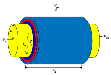
We proposed the analytical models to analyze shifts in threshold voltage and drain induced barrier lowering (DIBL) when the stacked SiO2/high-k dielectric was used as the oxide film of Junctionless Cylindrical Surrounding Gate (JLCSG) MOSFET. As a result of comparing the results of the presented model with those of TCAD, it was a good fit, thus proving the validity of the presented model. It could be found that the threshold voltage increased, but DIBL decreased by these models as the high-k dielectric constant increased. However, the shifts of threshold voltage and DIBL significantly decreased as the high-k dielectric constant increased. As for the degree of reduction, the channel length had a greater effect than the thickness of the high-k dielectric, and the shifts of threshold voltage and DIBL were kept almost constant when the high-k dielectric constant was 20 or higher. Therefore, the use of dielectrics such as HfO2/ZrO2, La2O3, and TiO2 with a dielectric constant of 20 or more for stacked oxide will be advantageous in reducing the short channel effect. In conclusion, these models were able to sufficiently analyze the threshold voltage and DIBL.
Citation: Hakkee Jung. Analytical models of threshold voltage and drain induced barrier lowering in junctionless cylindrical surrounding gate (JLCSG) MOSFET using stacked high-k oxide[J]. AIMS Electronics and Electrical Engineering, 2022, 6(2): 108-123. doi: 10.3934/electreng.2022007
We proposed the analytical models to analyze shifts in threshold voltage and drain induced barrier lowering (DIBL) when the stacked SiO2/high-k dielectric was used as the oxide film of Junctionless Cylindrical Surrounding Gate (JLCSG) MOSFET. As a result of comparing the results of the presented model with those of TCAD, it was a good fit, thus proving the validity of the presented model. It could be found that the threshold voltage increased, but DIBL decreased by these models as the high-k dielectric constant increased. However, the shifts of threshold voltage and DIBL significantly decreased as the high-k dielectric constant increased. As for the degree of reduction, the channel length had a greater effect than the thickness of the high-k dielectric, and the shifts of threshold voltage and DIBL were kept almost constant when the high-k dielectric constant was 20 or higher. Therefore, the use of dielectrics such as HfO2/ZrO2, La2O3, and TiO2 with a dielectric constant of 20 or more for stacked oxide will be advantageous in reducing the short channel effect. In conclusion, these models were able to sufficiently analyze the threshold voltage and DIBL.

| [1] |
Afzalian A (2021) Ab initio perspective of ultra-scaled CMOS from 2D-material fundamentals to dynamically doped transistors. npj 2D Mater Appl 5: 1-13. https://doi.org/10.1038/s41699-020-00181-1 doi: 10.1038/s41699-020-00190-0

|
| [2] |
Xu K, Chen D, Yang F, et al. (2017) Sub-10 nm Nanopattern Architecture for 2D Material Field-Effect Transistor. Nano Lett 17: 1065-1070. https://doi.org/10.1021/acs.nanolett.6b04576 doi: 10.1021/acs.nanolett.6b04576
|
| [3] |
Menduratta N, Tripathi SL (2020) A review on performance comparison of advanced MOSFET structures below 45 nm technology node. J Semicond 41: 061401. https://doi.org/10.1088/1674-4926/41/6/061401 doi: 10.1088/1674-4926/41/6/061401
|
| [4] |
Lee J, Choi K (2016) Trend and issues of the bulk FinFET. Vacuum Magazine 3: 16-21. https://doi.org/10.5757/vacmac.3.1.16 doi: 10.5757/vacmac.3.1.16
|
| [5] | Chiarella T, Kubicek S, Rosseel E, et al. (2016) Towards High Performance Sub-10 nm finW Bulk FinFET Technology. 2016 46th European Solid-State Device Research Conference (ESSDERC), Lausanne Switzerland, 131-134. https://doi.org/10.1109/ESSDERC.2016.7599605 |
| [6] |
Zhao D, Tian Z, Liu H, et al. (2020) Realizing an Omega-Shaped Gate MoS2 Field-Effect Transistor Based on a SiO2/MoS2 Core-Shell Heterostructure. ACS Appl Mater Inter 12: 14308-14314. https://doi.org/10.1021/acsami.9b21727 doi: 10.1021/acsami.9b21727
|
| [7] |
Agarwal A, Pradhan PC, Swain BP (2020) Corrected Drain Current Model for Schottky Barrier Cylindrical Gate All Around FET Considering Quantum Mechanical Effects. Telecommunications and Radio Engineering 79: 433-442. https://doi.org/10.1615/TelecomRadEng.v79.i5.60 doi: 10.1615/TelecomRadEng.v79.i5.60
|
| [8] | Dargar A, Srivastava VM (2021) Performance Comparison of Stacked Dual-Metal Gate Engineered Cylindrical Surrounding Double-Gate MOSFET. Int J Electron Telec 67: 29-34. |
| [9] | Sharma S, Chaudhury K (2012) A Novel Technique for Suppression of Corner Effect in Square Gate All Around MOSFET. Electrical and Electronic Engineering 2: 336-341. |
| [10] |
Lee J, Kang M (2021) TID Circuit Simulation in Nanowire FETs and Nanosheet FETs. Electronics 10: 956. https://doi.org/10.3390/electronics10080956 doi: 10.3390/electronics10080956
|
| [11] |
Colinge JP, Kranti A, Yan R, et al. (2011) Junctionless Nanowire Transistor (JNT): Properties and design guidelines. Solid-State Electronics 65: 33-37. https://doi.org/10.1016/j.sse.2011.06.004 doi: 10.1016/j.sse.2011.06.004
|
| [12] |
Nowbahari A, Roy A, Marchetti L (2020) Junctionless Transistors: State-of-the-Art. Electronics 9: 1174. https://doi.org/10.3390/electronics9071174 doi: 10.3390/electronics9071174
|
| [13] |
Lee C, Borne A, Ferain I, et al. (2010) High-Temperature Performance of Silicon Junctionless MOSFETs. IEEE T Electron Dev 57: 620-625. https://doi.org/10.1109/TED.2009.2039093 doi: 10.1109/TED.2009.2039093
|
| [14] | Huda ARN, Arshad MKM, Othman N, et al. (2015) Impact of Size Variation in Junctionless vs Junction Planar SOI n-MOSFET Transistor. 2015 IEEE Regional Symposium on Micro and Nanoelectronics(RSM), Kuala Terengganu, 1-4. https://doi.org/10.1109/RSM.2015.7354983 |
| [15] |
Jung H (2019) Analysis of Threshold Voltage Roll-off and Drain Induced Barrier Lowering in Junction-Based and Junctionless Double Gate MOSFET. Journal of the Korean Institute of Electrical and Electronic Material Engineers 32: 104-109. https://doi.org/10.21660/2019.55.4510 doi: 10.21660/2019.55.4510
|
| [16] |
Jung H (2021) Analysis of subthreshold swing in junctionless double gate MOSFET using stacked high-k gate oxide. International Journal of Electrical and Computer Engineering 11: 240-248. https://doi.org/10.11591/ijece.v11i1.pp240-248 doi: 10.11591/ijece.v11i1.pp240-248
|
| [17] |
Manikanda S, Balamurugan NB, Nirmal D (2020) Analytical Model of Double Gate Stacked Oxide Junctionless Transistor Considering Source/Drain Depletion Effetcs for CMOS Low Power Application. Silicon 12: 2053-2063. https://doi.org/10.1007/s12633-019-00280-9 doi: 10.1007/s12633-019-00280-9
|
| [18] |
Haque M, Kabir H, Adnan MR (2021) Analytical modelling and verification of potential profile of DG JLFET with and without stack oxide. Int J Electron 108: 819-840. https://doi.org/10.1080/00207217.2020.1818842 doi: 10.1080/00207217.2020.1818842
|
| [19] |
Baral K, Singh PK, Kumar S, et al. (2020) Ultrathin body nanowire hetero-dielectric stacked asymmetric halo doped junctionless accumulation model MOSFET for enhanced electrical chracteristics and negative bias stability. Superlattice Microst 138: 106364. https://doi.org/10.1016/j.spmi.2019.106364 doi: 10.1016/j.spmi.2019.106364
|
| [20] |
Swain SK, Biswal SM, Das SK, et al. (2020) Performance Comparison of InAs Based DG-MOSFET with Respect to SiO2 and Gate Stack Configuration. Nanoscience & Nanotechnology-Asia 10: 419-424. https://doi.org/10.2174/2210681209666190919094434 doi: 10.2174/2210681209666190919094434
|
| [21] |
Panchanan S, Maity R, Maity NP (2021) Modeling, Simulation and Analysis of Surface Potential and Threshold Voltage: Application to High-K Material HfO2 Based FinFET. Silicon 13: 3271-3289. https://doi.org/10.1007/s12633-020-00607-x doi: 10.1007/s12633-020-00607-x
|
| [22] |
Maity NP, Maity R, Maity S, et al (2019) A New Surface Potential and Drain Current Model of Dual Material Gate Short Channel Metal Oxide Semiconductor Field Effect Transistor in Subthreshold Regime: Application to High-K material HfO2. J Nanoelectron Optoe 14: 868-876. https://doi.org/10.1166/jno.2019.2547 doi: 10.1166/jno.2019.2547
|
| [23] | Rasol MFM, Hamid FKA, Johari Z, et al. (2019) Stacking SiO2/High-k Dielectric Material in 30 nm Junction-less Nanowire Transistor Optimized Using Taguchi Method for Lower Leakage Current. 2019 IEEE Regional Symposium on Micro and Nanoelectronics (RSM), Pahang, 1-4. https://doi.org/10.1109/RSM46715.2019.8943545 |
| [24] |
Darwin S, Samuel TSA, Vimala P (2020) Impact of two gate oxide with no junction metal oxide semiconductor field effect transistor- an analytical model. Physica E: Low-dimensional Systems and Nanostructures 118: 113803. https://doi.org/10.1016/j.physe.2019.113803 doi: 10.1016/j.physe.2019.113803
|
| [25] | Kosmani NF, Mamid FA, Razali MA (2020) Effect of High-k Dielectric Materials on Electrical Performance on Double Gate and Gate-All-Around MOSFET. Int J Integ Eng 12: 81-88. |
| [26] | Gupta S, Pandey N., Gupta RS (2020) Investigation of Dual-Material Double Gate Junctionless Accumulation-Mode Cylindrical Gate All Around(DMDG-JLAM-CGAA) MOSFET with High-k Gate Stack for Low Power Digital Applications. 2020 IEEE 17th india Council International Conference (INDICON), New Delhi 1-4. https://doi.org/10.1109/INDICON49873.2020.9342380 |
| [27] |
Gupta V, Awasthi H, Kumar N et al. (2021) A Novel Approach to Model Threshold Voltage and Subthreshold Current of Graded-Doped Junctionless-Gate-All-Around(GD-JL-GAA) MOSFETs. Silicon 1-9. https://doi.org/10.1007/s12633-021-01084-6 doi: 10.1007/s12633-021-01084-6
|
| [28] |
Hu G, Xiang P, Ding Z, et al. (2014) Analytical Models for Electric Potential, Threshold Voltage, and Subthreshold Swing of Junctionless Surrounding-Gate Transistors. IEEE T Electron Dev 61: 688-695. https://doi.org/10.1109/TED.2013.2297378 doi: 10.1109/TED.2013.2297378
|
| [29] |
Maduagwu UA, Srivastava VM (2019) Analytical Performance of the Threshold Voltage and Subthreshold Swing of CSDG MOSFET. Journal of Low Power Electronics and Applications 9: 10. https://doi.org/10.3390/jlpea9010010 doi: 10.3390/jlpea9010010
|
| [30] |
Li C, Zhuang Y, Di S., et al. (2013) Subthreshold Behavior Models for Nanoscale Short-Channel Junctionless Cylindrical Surrounding-Gate MOSFETs. IEEE T Electron Dev 60: 3655-3662. https://doi.org/10.1109/TED.2013.2281395 doi: 10.1109/TED.2013.2281395
|
| [31] |
Duksh YS, Singh B, Gola D, et al. (2021) Subthreshold Modeling of Graded Channel Double Gate Junctionless FETs. Silicon 13: 1231-1238. https://doi.org/10.1007/s12633-020-00514-1 doi: 10.1007/s12633-020-00514-1
|
| [32] |
Gupta SK (2015) Threshold voltage model of junctionless cylindrical surrounding gate MOSFETs including fringing field effects. Supperlattices and Microstructures 88: 188-197. https://doi.org/10.1016/j.spmi.2015.09.001 doi: 10.1016/j.spmi.2015.09.001
|
| [33] | Ehteshanuddin M, Loan SA, Rafat M (2017) Excellent DIBL Immunity in Junctionless Transistor on a High-k Buried Oxide. 2017 IEEE 14th india Council International Conference (INDICON), Roorke, 1-4. https://doi.org/10.1109/INDICON.2017.8487497 |
| [34] |
Bhagat K, Patil GC (2020) Engineering substrate doping in bulk planar junctionless transistor: Scalability and variability study. Engineering Research Express 2: 025028. https://doi.org/10.1088/2631-8695/ab91f7 doi: 10.1088/2631-8695/ab91f7
|
| [35] |
Lagraf F, Rechem D, Guergouri K, et al. (2019) Channel Length Effect on Subthreshold Characteristics of Junctionless Trial Material Cylindrical Surrounding-Gate MOSFET with High-k Gate Dielectrics. Journal of Nano- and Electronic Physics 11: 02011. https://doi.org/10.21272/jnep.11(2).02011 doi: 10.21272/jnep.11(2).02011
|
| [36] |
Clark RD (2014) Emerging Applications for High K Materials in VLSI Technology. Materials 7: 2913-2944. https://doi.org/10.3390/ma7042913 doi: 10.3390/ma7042913
|


Figures(9) / Tables(1)

Hakkee Jung. Analytical models of threshold voltage and drain induced barrier lowering in junctionless cylindrical surrounding gate (JLCSG) MOSFET using stacked high-k oxide[J]. AIMS Electronics and Electrical Engineering, 2022, 6(2): 108-123. doi: 10.3934/electreng.2022007


 DownLoad: