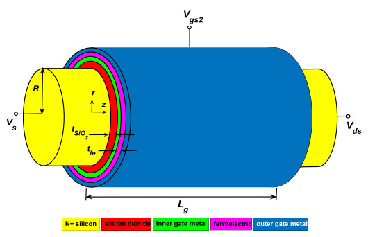
An analytical SS model is presented to observe the subthreshold swing (SS) of a junctionless gate-all-around (GAA) FET with ferroelectric in this paper. For the gate structure, a multilayer structure of metal-ferroelectric-metal-insulator-semiconductor (MFMIS) was used, and the SS was calculated in $15 \leqslant {P_r} \leqslant 30\,\mu C/c{m^2}$ and $0.8 \leqslant {E_c} \leqslant 1.5\,MV/cm$, which are the ranges of remanent polarization and coercive field suggested in various experiments in the case of HZO as the ferroelectric material. It was found that the SSs from the presented analytical SS model agree well with those derived from the relationship between drain current and gate voltage using a 2D potential distribution in the range of device parameters used for simulation. As a result of analyzing the SS of the junctionless GAA FET with ferroelectric using the analytical SS model presented in this paper, the SS decreased because the voltage across the inner gate decreased when the ferroelectric thickness increased. It was observed that the condition of SS < 60 mV/dec was sufficiently obtained according to changes in device parameters such as channel length, channel radius and ferroelectric thickness, and that the SS maintained a constant value according to the ratio of remanent polarization and coercive field Pr/Ec. As Pr/Ec increases, the SS increases as the ferroelectric capacitance increases. As the channel length becomes smaller, the change in SS according to Pr/Ec is more severe.
Citation: Hakkee Jung. Analytical model of subthreshold swing in junctionless gate-all-around (GAA) FET with ferroelectric[J]. AIMS Electronics and Electrical Engineering, 2023, 7(4): 322-336. doi: 10.3934/electreng.2023017
An analytical SS model is presented to observe the subthreshold swing (SS) of a junctionless gate-all-around (GAA) FET with ferroelectric in this paper. For the gate structure, a multilayer structure of metal-ferroelectric-metal-insulator-semiconductor (MFMIS) was used, and the SS was calculated in $15 \leqslant {P_r} \leqslant 30\,\mu C/c{m^2}$ and $0.8 \leqslant {E_c} \leqslant 1.5\,MV/cm$, which are the ranges of remanent polarization and coercive field suggested in various experiments in the case of HZO as the ferroelectric material. It was found that the SSs from the presented analytical SS model agree well with those derived from the relationship between drain current and gate voltage using a 2D potential distribution in the range of device parameters used for simulation. As a result of analyzing the SS of the junctionless GAA FET with ferroelectric using the analytical SS model presented in this paper, the SS decreased because the voltage across the inner gate decreased when the ferroelectric thickness increased. It was observed that the condition of SS < 60 mV/dec was sufficiently obtained according to changes in device parameters such as channel length, channel radius and ferroelectric thickness, and that the SS maintained a constant value according to the ratio of remanent polarization and coercive field Pr/Ec. As Pr/Ec increases, the SS increases as the ferroelectric capacitance increases. As the channel length becomes smaller, the change in SS according to Pr/Ec is more severe.

| [1] |
Ratnesh RK, Goel A, Kaushik G, Garg H, Singh M, Prasad B (2021) Advancement and challenges in MOSFET scaling. Mat Sci Semicon Proc 134: 106002. https://doi.org/10.1016/j.mssp.2021.106002 doi: 10.1016/j.mssp.2021.106002

|
| [2] |
Khanna VK (2016) Short-Channel Effects in MOSFETs. Integrated Nanoelectronics: Nanoscale CMOS, Post-CMOS and Allied Nanotechnologies, 73‒93. https://doi.org/10.1007/978-81-322-3625-2_5 doi: 10.1007/978-81-322-3625-2_5
|
| [3] |
Zhang S (2020) Review of Modern Field Effect Transistor Technologies for Scaling. Journal of Physics: Conference Series 1617: 012054. https://doi.org/10.1088/1742-6596/1617/1/012054 doi: 10.1088/1742-6596/1617/1/012054
|
| [4] |
Razavieh A, Zeitzoff P, Nowak EJ (2019) Challenges and Limitations of CMOS Scaling for FinFET and Beyond Architectures. IEEE T Nanotechnol 18: 999‒1004. https://doi.org/10.1109/TNANO.2019.2942456 doi: 10.1109/TNANO.2019.2942456
|
| [5] |
Saini G, Rana AK (2011) Physical Scaling Limits of FinFET Structure: A Simulation Study. International Journal of VLSI & Communication Systems 2: 26‒35. https://doi.org/10.5121/vlsic.2011.2103 doi: 10.5121/vlsic.2011.2103
|
| [6] |
Hu VP, Chiu P, Sachid AB, Hu C (2017) Negative Capacitance Enables FinFET and FDSOI Scaling to 2 nm Node. Electron Devices Meeting (IEDM) 23.1.1‒23.1.4. https://doi.org/10.1109/IEDM.2017.8268443 doi: 10.1109/IEDM.2017.8268443
|
| [7] |
Chauhan V, Samajdar DP (2021) Recent Advances in Negative Capacitance FinFETs for Low-Power Applications: A Review. IEEE T Ultrason Ferr 68: 3056‒3068. https://doi.org/10.1109/TUFFC.2021.3095616 doi: 10.1109/TUFFC.2021.3095616
|
| [8] |
Yan S, Wu C, Sun C, Lin YW, Yao YJ, Wu YC. (2022) Trench FinFET Nanostructure with Advanced Ferroelectric Nanomaterial HfZrO2 for Sub-60-mV/Decade Subthreshold Slope for Low Power Application. Nanomaterials 12: 2165. https://doi.org/10.3390/nano12132165 doi: 10.3390/nano12132165
|
| [9] |
Mukesh S, Zhang J (2022) A Review of the Gate-All-Around Nanosheet FET Process Opportunities. Electronics 11: 3589. https://doi.org/10.3390/electronics11213589 doi: 10.3390/electronics11213589
|
| [10] |
Qin L, Li C, Wei Y, Hu G, Chen J, Li Y, et al. (2023) Recent Developments in Negative Capacitance Gate-All-Around Field Effect Transistors: A Review. IEEE Access 11: 14028‒14042. https://doi.org/10.1109/ACCESS.2023.3243697 doi: 10.1109/ACCESS.2023.3243697
|
| [11] | Shilov A (2022) Samsung Begins 3 nm Production: World's First Gate-All-Around Transistors. Available from: https://www.tomshardware.com/news/samsung-kicks-off-3nm-production-gate-all-around-fets-make-an-entrance |
| [12] |
Batakala J, Dhar RS (2022) Effect of Channel Material on Performance Parameters of GAA MOSFET. Journal of Nano- and Electronic Physics 14: 02003. https://doi.org/10.21272/jnep.14(2).02003 doi: 10.21272/jnep.14(2).02003
|
| [13] | Jazaeri F, Sallese JM (2018) Modeling nanowire and double-gate junctionless field-effect transistors, Cambridge University Press. https://doi.org/10.1017/9781316676899 |
| [14] |
Colinge JP, Lee CW, Afzalian A, Akhavan ND, Yan R, Ferain I, et al. (2010) Nanowire transistors without junctions. Nature Nanotech 5: 225‒229. https://doi.org/10.1038/nnano.2010.15 doi: 10.1038/nnano.2010.15
|
| [15] |
Chaujar R, Yirak MG (2023) Sensitivity Investigation of Junctionless Gate-all-around Silicon Nanowire Field-Effect Transistor-Based Hydrogen Gas Sensor. Silicon 15: 609‒621. https://doi.org/10.1007/s12633-022-02242-0 doi: 10.1007/s12633-022-02242-0
|
| [16] |
Priyadarshani KN, Singh S, Mohammed MKA (2022) Gate-all-around junctionless FET based label-free dielectric/charge modulation detection of SARS-CoV-2 virus. RSC Advances 12: 9202‒9209. https://doi.org/10.1039/d1ra08587e doi: 10.1039/d1ra08587e
|
| [17] |
Merad F, Guen-Bouazza A (2020) DC performance analysis of a 20 nm gate length n-type Silicon GAA junctionless (Si JL-GAA) transistor. International Journal of Electrical and Computer Engineering 10: 4043‒4052. https://doi.org/10.11591/ijece.v10i4.pp4043-4052 doi: 10.11591/ijece.v10i4.pp4043-4052
|
| [18] |
Lee S, Chen H, Shen C, Kuo PY, Chung CC, Huang YE, et al. (2020) Effect of Seed Layer on Gate-All-Around Poly-Si Nanowire Negative-Capacitance FETs With MFMIS and MFIS Structures: Planar Capacitors to 3-D FETs. IEEE T Electron Dev 67: 711‒716. https://doi.org/10.1109/TED.2019.2958350 doi: 10.1109/TED.2019.2958350
|
| [19] | Lee S, Chen H, Shen C, Kuo PY, Chung CC, Huang YE, et al. (2019) Experimental Demonstration of Performance Enhancement of MFMIS and MFIS for 5-nmx12.5-nm Poly-Si Nanowire Gate-All-Around Negative Capacitance FETs Featuring Seed-Layer and PMA-Free Process. 2019 Silicon Nanoelectronics Workshop (SNW), 1‒2. https://doi.org/23919/SNW.2019.8782939 |
| [20] |
Sakib FI, Mullick FE, Shahnewaz S, Islam S, Hossain M (2020) Influence of device architecture on the performance of negative capacitance MFMIS transistors. Semicond Sci Technol 35: 025005. https://doi.org/10.1088/1361-6641/ab5b76 doi: 10.1088/1361-6641/ab5b76
|
| [21] |
Thoti N, Li Y (2022) Design of GAA Nanosheet Ferroelectric Area Tunneling FET and Its Significance with DC/RF Characteristics Including Linearity Analyses. Nanoscale Res Lett 17: 53. https://doi.org/10.1186/s11671-022-03690-8 doi: 10.1186/s11671-022-03690-8
|
| [22] |
Rassekh A, Sallese J, Jazaeri F, Fathipour M, Ionescu AM (2020) Negative Capacitance Double-Gate Junctionless FETs: A Charge-Based Modeling Investigation of Swing, Overdrive and Short Channel Effect. IEEE J Electron Devi 8: 939‒947. https://doi.org/10.1109/JEDS.2020.3020976 doi: 10.1109/JEDS.2020.3020976
|
| [23] |
Pahwa G, Agarwal A, Chauhan YS (2018) Numerical Investigation of Short-Channel Effects in Negative Capacitance MFIS and MFMIS Transistors: Subthreshold Behavior. IEEE T Electron Dev 65: 5130‒5136. https://doi.org/109/TED.2018.2870519 doi: 10.1109/TED.2018.2870519
|
| [24] |
Sakib FI, Hasan MA, Hossain M (2020) Exploration of Negative Capacitance in Gate-All-Around Si Nanosheet Transistors. IEEE T Electron Dev 67: 5236‒5242. https://doi.org/10.1109/TED.2020.3025524 doi: 10.1109/TED.2020.3025524
|
| [25] |
Raut P, Nanda U, Panda DK (2022) RF with linearity and non-linearity parameter analysis of gate all around negative capacitance junction less FET (GAA-NC-JLFET) for different ferroelectric thickness. Phys Scripta 97: 105809. https://doi.org/10.1088/1402-4896/ac90fa doi: 10.1088/1402-4896/ac90fa
|
| [26] |
Choi Y, Hong Y, Shin C (2020) Device design guideline for junctionless gate-all-around nanowire negative-capacitance FET with HfO2-based ferroelectric gate stack. Semicond Sci Technol 35: 015011. https://doi.org/10.1088/1361-6641/ab5775 doi: 10.1088/1361-6641/ab5775
|
| [27] |
Mehta H, Kaur H (2017) Impact of interface layer and metal workfunction on device performance of ferroelectric junctionless cylindrical surrounding gate transistors. Superlattices and Microstructures 111: 194‒205. https://doi.org/10.1016/j.spmi.2017.06.032 doi: 10.1016/j.spmi.2017.06.032
|
| [28] |
Gaidhane AD, Pahwa G, Verma A, Chauhan YS (2018) Compact Modeling of Drain Current, Charges and Capacitances in Long-Channel Gate-All-Around Negative Capacitance MFIS Transistor. IEEE T Electron Dev 65: 2024‒2032. https://doi.org/10.1109/TED.2018.2813059 doi: 10.1109/TED.2018.2813059
|
| [29] |
Kim Y, Seon Y, Kim S, Kim J, Bae S, Yang I, et al. (2021) Analytical Current-Voltage Modeling and Analysis of the MFIS Gate-All-Around Transistor Featuring Negative-Capacitance. Electronics 10: 1177. https://doi.org/10.3390/electronics10101177 doi: 10.3390/electronics10101177
|
| [30] |
Lee S, Lee C, Kuo Y, Li S, Chao T (2021) Ultra Sub-5-nm Hf1-xZrxO2 for a Stacked Gate-All-Around Ferroelectric FET With Internal Metal Gate. Journal of the Electron Devices Society 9: 236‒241. https://doi.org/10.1109/JEDS.2021.3056438 doi: 10.1109/JEDS.2021.3056438
|
| [31] |
Zhao G, Wang X, Yip WH, Huy NTV, Coquet P, Haung M, et al. (2022) Ternary logics based on 2D ferroelectric-incorporated 2D semiconductor field effect transistors. Front Mater 9: 872909. https://doi.org/10.3389/fmats.2022.872909 doi: 10.3389/fmats.2022.872909
|
| [32] |
Li C, Zhaung Y, Di S, Han R (2013) Subthreshold Behavior Models for Nanoscale Short-Channel Junctionless Cylindrical Surrounding-Gate MOSFETs. IEEE T Electron Dev 60: 3655‒3662. https://doi.org/10.1109/TED.2013.2281395 doi: 10.1109/TED.2013.2281395
|
| [33] |
Das D, Gaddam V, Jeon S (2020) Demonstration of High Ferroelectricity (Pr~29μC/cm2) in Zr Rich HfxZr1-O2 Films. IEEE Electron Device Letters 41: 34‒37. https://doi.org/10.1109/LED.2019.2955198 doi: 10.1109/LED.2019.2955198
|
| [34] |
Das D, Buyantogtokh B, Gaddam V, Jeon S (2021) Influence of High-Pressure Annealing Conditions on Ferroelectric and Interfacial Properties of Zr-rich HfxZr1-xO2 Capacitors. IEEE T Electron Dev 68: 1996‒2002. https://doi.org/10.1109/TED.2021.3061963 doi: 10.1109/TED.2021.3061963
|
| [35] |
Chen K, Chen P, Wu Y (2017) Excellent reliability of ferroelectric HfZrOx free from wake-up and fatigue effects by NH3 plasma treatment. 2017 Symposium on VLSI Circuits, T84‒T85. https://doi.org/10.23919/VLSIC.2017.8008572 doi: 10.23919/VLSIC.2017.8008572
|
| [36] |
Dang Z, Lv S, Gao Z, Chen M, Xu Y, Jiang P, et al. (2022) Improved Endurance of Hf0.5Zr0.5O2-based Ferroelectric Capacitor Through Optimizing the Ti-N Ratio in TiN Electrode. Electron Device Letters 43: 561‒564. https://doi.org/10.1109/LED.2022.3153063 doi: 10.1109/LED.2022.3153063
|
| [37] |
Jung H (2022) Analysis of subthreshold swing in junctionless cylindrical surrounding gate MOSFET using Gaussian doping profile. International Journal of Advanced Technology and Engineering Exploration 9: 1073‒1082. https://doi.org/10.19101/IJATEE.2021.874994 doi: 10.19101/IJATEE.2021.874994
|
| [38] |
Tu L, Wang X, Wang J, Meng X, Chu J (2018) Ferroelectric Negative Capacitance Field Effect Transistor. Adv Electron Mater 4: 1800231. https://doi.org/10.1002/aelm.201800231 doi: 10.1002/aelm.201800231
|
| [39] |
Shafizade D, Shalchian M, Jazaeri F (2019) Ultrathin Junctionless Nanowire FET Model, Including 2-D Quantum Confinements. IEEE T Electron Dev 66: 4101‒4106. https://doi.org/10.1109/TED.2019.2930533 doi: 10.1109/TED.2019.2930533
|
| [40] |
Tamersit K, Jooq MKQ, Moaiyeri MH (2021) Analog/RF performance assessment of ferroelectric junctionless carbon nanotube FETs: A quantum simulation study. Physica E: Low-dimensional Systems and Nanostructures 134: 114915. https://doi.org/10.1016/j.physe.2021.114915 doi: 10.1016/j.physe.2021.114915
|
| [41] |
Pandey N, Pahwa G, Chauhan YS (2021) Addressing source to drain tunneling in extremely scaled Si-transistors using negative capacitance. Solid State Electron 186: 108189. https://doi.org/10.1016/j.sse.2021.108189 doi: 10.1016/j.sse.2021.108189
|
| [42] |
Kumar N, Purwar V, Awasthi H, Gupta R, Singh K, Dubey S (2021) Modeling the threshold voltage of core-and-outer gates of ultra-thin nanotube Junctionless-double gate-all-around (NJL-DGAA) MOSFETs. Microelectron J 113: 105104. https://doi.org/10.1016/j.mejo.2021.105104 doi: 10.1016/j.mejo.2021.105104
|
| [43] |
Kumar A, Tiwari PK, Roy JN (2022) Subthreshold model of asymmetric GAA junctionless FETs with scaled equivalent oxide thickness. Microelectron J 126: 105490. https://doi.org/10.1016/j.mejo.2022.105490 doi: 10.1016/j.mejo.2022.105490
|


Figures(9) / Tables(1)

Hakkee Jung. Analytical model of subthreshold swing in junctionless gate-all-around (GAA) FET with ferroelectric[J]. AIMS Electronics and Electrical Engineering, 2023, 7(4): 322-336. doi: 10.3934/electreng.2023017


 DownLoad: