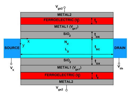
We analyze the drain induced barrier lowering (DIBL) of a negative capacitance (NC) FET using a gate structure such as a metal-ferroelectric-metal-insulator-semiconductor (MFMIS) for a junctionless double gate (JLDG) FET. NC FETs show negative DIBL characteristics according to the ferroelectric thickness. To elucidate the cause of such negative DIBL, the DIBLs are obtained by the second derivative method using the 2D potential distribution and drain current-gate voltage curve. The analytical DIBL model is also presented for easy observation of the DIBL of NC FET. It has been found that the results of this analytical DIBL model are very similar to those of the second derivative method. The results of this analytical DIBL model are also in good agreement with the results of TCAD. As a result, it was found that the negative DIBL phenomenon is caused by the change according to the drain voltage of the charge existing in the ferroelectric material. The negative DIBL phenomenon easily occurred as the ferroelectric thickness increased and the thickness of SiO2 used as an insulator decreases.
Citation: Hakkee Jung. Analysis of drain induced barrier lowering for junctionless double gate MOSFET using ferroelectric negative capacitance effect[J]. AIMS Electronics and Electrical Engineering, 2023, 7(1): 38-49. doi: 10.3934/electreng.2023003
We analyze the drain induced barrier lowering (DIBL) of a negative capacitance (NC) FET using a gate structure such as a metal-ferroelectric-metal-insulator-semiconductor (MFMIS) for a junctionless double gate (JLDG) FET. NC FETs show negative DIBL characteristics according to the ferroelectric thickness. To elucidate the cause of such negative DIBL, the DIBLs are obtained by the second derivative method using the 2D potential distribution and drain current-gate voltage curve. The analytical DIBL model is also presented for easy observation of the DIBL of NC FET. It has been found that the results of this analytical DIBL model are very similar to those of the second derivative method. The results of this analytical DIBL model are also in good agreement with the results of TCAD. As a result, it was found that the negative DIBL phenomenon is caused by the change according to the drain voltage of the charge existing in the ferroelectric material. The negative DIBL phenomenon easily occurred as the ferroelectric thickness increased and the thickness of SiO2 used as an insulator decreases.

| [1] |
Chen M, Sun X, Liu H, et al. (2020) A FinFET with one atomic layer channel. Nat Commun 11: 1205. https://doi.org/10.1038/s41467-020-15096-0 doi: 10.1038/s41467-020-15096-0

|
| [2] |
Maurya RK, Bhowmick B (2021) Review of FinFET Devices and Perspective on Circuit Design Challenges. Silicon 14: 5783-5791. https://doi.org/10.1007/s12633-021-01366-z doi: 10.1007/s12633-021-01366-z
|
| [3] |
Park J, Kim J, Showdhury S, et al. (2020) Electrical Characteristics of Bulk FinFET According to Spacer Length. Electronics, 9: 1283. https://doi.org/10.3390/electronics9081283 doi: 10.3390/electronics9081283
|
| [4] |
Vashishtha V, Clark LT (2021) Comparing bulk-Si FinFET and gate-all-around FETs for the 5 nm technology node. Microelectron J 107: 104942. https://doi.org/10.1016/j.mejo.2020.104942 doi: 10.1016/j.mejo.2020.104942
|
| [5] |
Kim S, Kim J, Jang D, et al. (2020) Comparison of Temperature Dependent Carrier Transport in FinFET and Gate-All-Around Nanowire FET. Applied Sciences 10: 2979. https://doi.org/10.3390/app10082979 doi: 10.3390/app10082979
|
| [6] |
Agarwal A, Pradhan PC, Swain BP (2019) Effects of the physical parameter on gate all around FET. Sadhana 44: 248. https://doi.org/10.1007/s12046-019-1232-8 doi: 10.1007/s12046-019-1232-8
|
| [7] |
Ma J, Chen X, Sheng Y, et al. (2022) Top gate engineering of field-effect transistors based on wafer-scale two-dimensional semiconductors. J Mater Sci Technol 106: 243-248. https://doi.org/10.1016/j.jmst.2021.08.021 doi: 10.1016/j.jmst.2021.08.021
|
| [8] |
Karbalaei M, Dideban D, Heidari H (2021) A sectorial scheme of gate-all-around field effect transistor with improved electrical characteristics. Ain Shams Eng J 12: 755-760. https://doi.org/10.1016/j.asej.2020.04.015 doi: 10.1016/j.asej.2020.04.015
|
| [9] |
Lee K, Park J (2021) Inner Spacer Engineering to Improve Mechanical Stability in Channel-Release Process of Nanosheet FETs. Electronics 10: 1395. https://doi.org/10.3390/electronics10121395 doi: 10.3390/electronics10121395
|
| [10] |
Saeidi A, Rosca T, Memisevic E, et al. (2020) Nanowire Tunnel FET with Simultaneously Reduced Subthermionic Subthreshold Swing and Off-Current due to Negative Capacitance and Voltage Pinning Effects. Nano Letters 20: 3255-3262. https://doi.org/10.1021/acs.nanolett.9b05356 doi: 10.1021/acs.nanolett.9b05356
|
| [11] |
Zhang M, Guo Y, Zhang J, et al. (2020) Simulation Study of the Double-Gate Tunnel Field-Effect Transistor with Step Channel Thickness. Nanoscale Res Lett 15: 128. https://doi.org/10.1186/s11671-020-03360-7 doi: 10.1186/s11671-020-03360-7
|
| [12] |
Cao W, Banerjee K (2020) Is negative capacitance FET a steep-slope logic switch? Nat Commun 11: 196. https://doi.org/10.1038/s41467-019-13797-9 doi: 10.1038/s41467-019-13797-9
|
| [13] |
Rahi SB, Tayal S, Upadhyay AK (2021) A review on emerging negative capacitance field effect transistor for low power electronics. Microelectron J 116: 105242. https://doi.org/10.1016/j.mejo.2021.105242 doi: 10.1016/j.mejo.2021.105242
|
| [14] |
Lukyanchuk I, Razumnaya A, Sene A, et al. (2022) The ferroelectric field-effect transistor with negative capacitance. NPJ Comput Mater 8: 52. https://doi.org/10.1038/s41524-022-00738-2 doi: 10.1038/s41524-022-00738-2
|
| [15] |
Lee MH, Wei YT, Huang JJ, et al. (2015) Ferroelectricity of HfZrO2 in Energy Landscape With Surface Potential Gain for Low-Power Steep-Slope Transistors. J Electron Devi Society 3: 377-381. https://doi.org/10.1109/JEDS.2015.2435492 doi: 10.1109/JEDS.2015.2435492
|
| [16] |
Alam MA, Si M, Ye PD (2019) A critical review of recent progress on negative capacitance field-effect transistors. Appl Phys Lett 114: 090401. https://doi.org/10.1063/1.5092684 doi: 10.1063/1.5092684
|
| [17] |
Li Y, Kang Y, Gong X (2017) Evaluation of Negative Capacitance Ferroelectric MOSFET for Analog Circuit Applications. IEEE T Electron Dev 64: 4317-4321. https://doi.org/10.1109/TED.2017.2734279 doi: 10.1109/TED.2017.2734279
|
| [18] |
Lee H, Yoon Y, Shin C (2017) Current-Voltage Model for Negative Capacitance Field-Effect Transistors. IEEE Electr Device L 38: 669-672. https://doi.org/10.1109/LED.2017.2679102 doi: 10.1109/LED.2017.2679102
|
| [19] |
Ortiz-Conde A, Garcia-Sanchez FJ, Muci J, et al. (2013) Revisiting MOSFET threshold voltage extraction methods. Microelectron Reliab 53: 90-104. https://doi.org/10.1016/j.microrel.2012.09.015 doi: 10.1016/j.microrel.2012.09.015
|
| [20] |
Chebaki E, Djeffal F, Bentrcia T (2012) Two-dimensional numerical analysis of nanoscale junctionless and conventional Double Gate MOSFETs including the effect of interfacial traps. Physica Status Solidi C 9: 2041-2044. https://doi.org/10.1002/pssc.201200128 doi: 10.1002/pssc.201200128
|
| [21] | Farzan J, Sallese JM (2018) Modeling Nanowire and Double-Gate Junctionless Field-Effect Transistors. Cambridge University Press. |
| [22] |
Shalchian M, Jazaeri F, Sallese JM (2018) Charge-Based Model for Ultrathin Junctionless DG FETs, Including Quantum Confinement. IEEE T Electron Dev 65: 4009-4014. https://doi.org/10.1109/TED.2018.2854905 doi: 10.1109/TED.2018.2854905
|
| [23] |
Woo J, Choi J, Choi Y (2013) Analytical Threshold Voltage Model of Junctionless Double-Gate MOSFETs With Localized Charges. IEEE T Electron Dev 60: 2951-2955. https://doi.org/10.1109/TED.2013.2273223 doi: 10.1109/TED.2013.2273223
|
| [24] | Dhiman G, Ghosh PK (2017) Threshold Voltage Modeling for Nanometer Scale Junction Less Double Gate MOSFET. International Journal of Applied Engineering Research 12: 1807-1810. |
| [25] |
Jiang C, Liang R, Wang J, Xu J (2015) A two-dimensional analytical model for short channel junctionless double-gate MOSFETs. AIP Adv 5: 057122. https://doi.org/10.1063/1.4821086 doi: 10.1063/1.4821086
|
| [26] | Hoffmann M, Pesic M, Slesazeck S, et al. (2017) Modeling and design considerations for negative capacitance field-effect transistors. 2017 Joint International EUROSOI Workshop and International Conference on Ultimate Integration on Silicon (EuroSOI-ULIS), 1-4. IEEE. https://doi.org/10.1109/ULIS.2017.7962577 |
| [27] |
Rassekh A, Sallese J, Jazaeri F, et al. (2020) Negative Capacitance DG Junctionless FETs: A Charge-based Modeling Investigation of Swing, Overdrive and Short Channel Effect. J Electron Devi Society 8: 939-947. https://doi.org/10.1109/JEDS.2020.3020976 doi: 10.1109/JEDS.2020.3020976
|
| [28] |
Jazaeri F, Barbut L, Koukab A, et al. (2013) Analytical model for ultra-thin body junctionless symmetric double gate MOSFETs in subthreshold regime. Solid-State Electron 82: 103-110. https://doi.org/10.1016/j.sse.2013.02.001 doi: 10.1016/j.sse.2013.02.001
|
| [29] |
Awadhiya B, Kondekar PN, Yadav S, et al. (2021) Insight into Threshold Voltage and Drain Induced Barrier Lowering in Negative Capacitance Field Effect Transistor. Trans Electr Electro Mater 22: 267-273. https://doi.org/10.1007/s42341-020-00230-y doi: 10.1007/s42341-020-00230-y
|
| [30] | Saha AK, Sharma P, Dabo I, et al. (2017) Ferroelectric transistor model based on self-consistent solution of 2D Poisson's, non-equilibrium Green's function and multi-domain Landau Khalatnikov equations. 2017 IEEE International Electron Devices Meeting (IEDM), 13-15. https://doi.org/10.1109/IEDM.2017.8268385 |
| [31] |
Lee J (2021) Unified Model of Shot Noise in the Tunneling Current in Sub-10 nm MOSFETs. Nanomaterials 11: 2759. https://doi.org/10.3390/nano11102759 doi: 10.3390/nano11102759
|
| [32] |
Ding Z, Hu G, Gu J, et al. (2011) An analytical model for channel potential and subthreshold swing of the symmetric and asymmetric double-gate MOSFETs. Microelectron J 42: 515-519. https://doi.org/10.1016/j.mejo.2010.11.002 doi: 10.1016/j.mejo.2010.11.002
|
| [33] |
Rassekh A, Jazaeri F, Sallese J (2022) Nonhysteresis Condition in Negative Capacitance Junctionless FETs. IEEE T Electron Dev 69: 820-826. https://doi.org/10.1109/TED.2021.3133193 doi: 10.1109/TED.2021.3133193
|
| [34] |
Khan AI, Radhakrishna U, Chatterjee K, et al. (2016) Negative Capacitance Behavior in a Leaky Ferroelectric. IEEE T Electron Dev 63: 4416-4422. https://doi.org/10.1109/TED.2016.2612656 doi: 10.1109/TED.2016.2612656
|
| [35] |
Rassekh, Jazaeri F, Sallese JM (2022) Design Space of Negative Capacitance in FETs. IEEE T Nanotechnol 21: 236-243. https://doi.org/10.1109/TNANO.2022.3174471 doi: 10.1109/TNANO.2022.3174471
|
| [36] |
Jung H (2021) Relationship of drain induced barrier lowering and top/bottom gate oxide thickness in asymmetric junctionless double gate MOSFET. International Journal of Electrical and Computer Engineering 11: 232-239. https://doi.org/10.11591/ijece.v11i1.pp232-239 doi: 10.11591/ijece.v11i1.pp232-239
|


Figures(8) / Tables(1)

Hakkee Jung. Analysis of drain induced barrier lowering for junctionless double gate MOSFET using ferroelectric negative capacitance effect[J]. AIMS Electronics and Electrical Engineering, 2023, 7(1): 38-49. doi: 10.3934/electreng.2023003


 DownLoad: