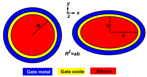
An analytical subthreshold swing (SS) model has been presented to determine the SS of an elliptic junctionless gate-all-around field-effect transistor (GAA FET). The analysis of a GAA FET with an elliptic cross-section is essential because it is difficult to manufacture a GAA FET with an accurate circular cross-section during the process. The SS values obtained using the proposed SS model were compared with 2D simulation values and other papers to confirm good agreement. Using this analytical SS model, SS was analyzed according to the eccentricity of the elliptic cross-section structure. As a result, it was found that the carrier control ability within the channel improved as the eccentricity increased due to a decrease in the effective channel radius by a decrease in the minor axis length and a decrease in the minimum potential distribution within the channel, and thus the SS decreased. There was no significant change in SS until the eccentricity increased to 0.75 corresponding to the aspect ratio (AR), the ratio of the minor and major axis lengths, of 1.5. However, SS significantly decreased when the eccentricity increased to 0.87 corresponding to AR = 2. As a result of the SS analysis for changes in the device parameters of the GAA FET, changes in the channel length, radius, and oxide film thickness significantly affected the changing rate of SS with eccentricity.
Citation: Hakkee Jung. Analytical subthreshold swing model of junctionless elliptic gate-all-around (GAA) FET[J]. AIMS Electronics and Electrical Engineering, 2024, 8(2): 211-226. doi: 10.3934/electreng.2024009
An analytical subthreshold swing (SS) model has been presented to determine the SS of an elliptic junctionless gate-all-around field-effect transistor (GAA FET). The analysis of a GAA FET with an elliptic cross-section is essential because it is difficult to manufacture a GAA FET with an accurate circular cross-section during the process. The SS values obtained using the proposed SS model were compared with 2D simulation values and other papers to confirm good agreement. Using this analytical SS model, SS was analyzed according to the eccentricity of the elliptic cross-section structure. As a result, it was found that the carrier control ability within the channel improved as the eccentricity increased due to a decrease in the effective channel radius by a decrease in the minor axis length and a decrease in the minimum potential distribution within the channel, and thus the SS decreased. There was no significant change in SS until the eccentricity increased to 0.75 corresponding to the aspect ratio (AR), the ratio of the minor and major axis lengths, of 1.5. However, SS significantly decreased when the eccentricity increased to 0.87 corresponding to AR = 2. As a result of the SS analysis for changes in the device parameters of the GAA FET, changes in the channel length, radius, and oxide film thickness significantly affected the changing rate of SS with eccentricity.

| [1] |
Dastgeer G, Shahzad ZM, Chae H, Kim YH, Ko BM, Eom J (2022) Bipolar Junction Transistor Exhibiting Excellent Output Characteristics with a Prompt Reponse against the Selective Protein. Adv Funct Mater 32: 2204781. https://doi.org/10.1002/adfm.202204781 doi: 10.1002/adfm.202204781

|
| [2] |
Dastgeer G, Nisar S, Rasheed A, Akbar K, Chavan VD, Kim DK, et al. (2024) Atomically engineered, high-speed non-volatile flash memory device exhibiting multibit data storage operations. Nano Energy 119: 109106. https://doi.org/10.1016/j.nanoen.2023.109106 doi: 10.1016/j.nanoen.2023.109106
|
| [3] | Hofman S (2022) What is a gate-all-around transistor? Available from: https://www.asml.com/en/news/stories/2022/what-is-a-gate-all-around-transistor |
| [4] |
Mukesh S, Zhang J (2022) A Review of the Gate-All-Around Nanosheet FET Process Opportunities. Electronics 11: 3589. https://doi.org/10.3390/electronics11213589 doi: 10.3390/electronics11213589
|
| [5] | Samsung Newsroom (2022) Samsung Begins Chip Production Using 3nm Process Technology with GAA Arhitecture. Available from: https://news.samsung.com/global/samsung-begins-chip-production-suing-3nm-process-technology-with-gaa-architecture |
| [6] | Shilov A (2022) TSMC Reveals 2nm Node: 30% More Performance by 2025. Available from: https://www.tomshardware.com/news/tsmc-reveals-2nm-fabrication-process |
| [7] |
Zhang Z, Lin Z, Liao P, Askarpour V, Dou H, Shang Z, et al. (2022) A Gate-All-Around In2O3 Nanoribbon FET With Near 20 mA/μm Drain Current. IEEE Electr Device Lett 43: 1905‒1908. https://doi.org/10.1109/LED.2022.3210005 doi: 10.1109/LED.2022.3210005
|
| [8] | Kumari T, Singh J, Tiwari PK (2021) Impact of Non-Rectangular Cross-Section on Electrical Performances of GAA FETs. 2021 IEEE 18th India Council International Conference (INDICON), 1‒6. https://doi.org/10.1109/INDICON52576.2021.9691574 |
| [9] |
Zhao F, Jia X, Luo H, Zhang J, Mao XT, Li Y, et al. (2023) Hybrid integrated Si nanosheet GAA-FET and stacked SiGe/Si FinFET using selective channel release strategy. Microelectronic Engineering 275: 111993. https://doi.org/10.1016/j.mee.2023.111993 doi: 10.1016/j.mee.2023.111993
|
| [10] |
Kumar S, Jha S (2013) Impact of elliptical cross-section on the propagation delay of multi-channel gate-all-around MOSFET based inverters. Microelectronics Journal 44: 844‒851. http://dx.doi.org/10.1016/j.mejo.2013.06.003 doi: 10.1016/j.mejo.2013.06.003
|
| [11] | Bangsaruntip S, Cohen GM, Majumdar A, Zhang Y, Engelmann SU, Fuller NC, et al. (2009) High Performance and Highly Uniform Gate-All-Around Silicon Nanowire MOSFETs with Wire Size Dependent Scaling. 2009 IEEE International Electron Device Meeting (IEDM), 1‒4. https://doi.org/10.1109/IEDM.2009.5424364 |
| [12] |
Liao Y, Chiang M, Kim K, Hsu W (2012) Assessment of structure variation in silicon nanowire FETs and impact on SRAM. Microelectronics Journal 43: 300‒304. http://dx.doi.org/10.1016/j.mejo.2011.12.002 doi: 10.1016/j.mejo.2011.12.002
|
| [13] | Mehta H, Kaur H (2016) High Temperature Performance Investigation of Elliptic Gate Ferroelectric Junctionless Transistor. 2016 3rd International Conference on Emerging Electronics (ICEE), 1‒4. https://doi.org/10.1109/ICEmElec.2016.8074588 |
| [14] |
Kumari A, Kumar S, Sharma TK, Das MK (2019) On the C-V characteristics of nanoscale strained gate-all-around Si/SiGe MOSFETs. Solid State Electronics 154: 36‒42. https://doi.org/10.1016/j.sse.2019.02.006 doi: 10.1016/j.sse.2019.02.006
|
| [15] | Chao P, Li Y (2014) Impact of Geometry Aspect Ratio on 10-nm Gate-All-Around Silicon-Germanium Nanowire Field Effect Transistors. IEEE 14th International Conference on Nanotechnology, 452‒455. https://doi.org/10.1109/NANO.2014.6968188 |
| [16] | Sharma TK, Kumar S (2017) Impact of Geometry Aspect Ratio on the Performance of Si GAA Nanowire MOSFET. 2017 International Conference on Microelectronic Devices, Circuits and Systems (ICMDCS), 1‒5. https://doi.org/10.1109/ICMDCS.2017.8211534 |
| [17] |
Zhang L, Li L, He J, Chan M (2011) Modeling Short-Channel Effect of Elliptical Gate-All-Around MOSFET by Effective Radius. IEEE Electron Device Letters 32: 1188‒1190. https://doi.org/10.1109/LED.2011.2159358 doi: 10.1109/LED.2011.2159358
|
| [18] |
Lee M, Park B, Cho I, Lee J (2012) Characteristics of Elliptical Gate-All-Around SONOS Nanowire with Effective Circular Radius. IEEE Electron Device Letters 33: 1613‒1615. https://doi.org/10.1109/LED.2012.2215303 doi: 10.1109/LED.2012.2215303
|
| [19] |
Saha P, Sarkar SK (2019) Drain current modeling of proposed dual material elliptical Gate-All-Around heterojunction TFET for enhanced device performance. Superlattices and Microstructures 130: 194‒207. https://doi.org/10.1016/j.spmi.2019.04.022 doi: 10.1016/j.spmi.2019.04.022
|
| [20] |
Chiang T (2021) Elliptical nanowire FET: Modeling the short-channel subthreshold current caused by interface-trapped-charge and its evaluation for subthreshold logic gate. Superlattices and Microstructures 149: 106751. https://doi.org/10.1016/j.spmi.2020.106751 doi: 10.1016/j.spmi.2020.106751
|
| [21] |
Kumar P, Koley K, Mech BC, Maurya A, Kumar S (2022) Analog and RF performance optimization for gate all around tunnel FET using broken-gap material. Scientific reports 12: 18254. https://doi.org/10.1038/s41598-022-22485-6 doi: 10.1038/s41598-022-22485-6
|
| [22] |
Kim S, Seo Y, Lee J, Kang M, Shin H (2018) GIDL analysis of the process variation effect in gate-all-around nanowire FET. Solid State Electronics 140: 59‒63. http://dx.doi.org/10.1016/j.sse.2017.10.017 doi: 10.1016/j.sse.2017.10.017
|
| [23] |
Li Y, Hwang C (2009) The effect of the geometry aspect ratio on the silicon ellipse-shaped surrounding-gate field-effect transistor and circuit. Semicond Sci Technol 24: 095018. https://doi.org/10.1088/0268-1242/24/9/095018 doi: 10.1088/0268-1242/24/9/095018
|
| [24] |
Jha S, Kumar A, Kumar S (2012) Impact of Elliptical Cross-Section on Some Electrical Properties of Gate-All-Around MOSFETs. Bonfring International Journal of Power Systems and Integrated Circuits 2: 18‒22. https://doi.org/10.9756/BIJPSIC.3139 doi: 10.9756/BIJPSIC.3139
|
| [25] |
Nowbahari A, Roy A, Marchetti L (2020) Junctionless Transistors: State-of-the-Art. Electronics 9: 1174. https://doi.org/10.3390/electronics9071174 doi: 10.3390/electronics9071174
|
| [26] |
Cherik IC, Abbasi A, Maity SK, Mohammadi S (2023) Junctionless tunnel field-effect transistor with a modified auxiliary gate, a novel candidate for high-frequency applications. Micro and Nanostructures 174: 207477. https://doi.org/10.1016/j.micrna.2022.207477 doi: 10.1016/j.micrna.2022.207477
|
| [27] |
Kaushal S, Rana AK (2023) Reliable and low power Negative Capacitance Junctionless FinFET based 6T SRAM cell. Integration 88: 313‒319. https://doi.org/10.1016/j.vlsi.2022.10.014 doi: 10.1016/j.vlsi.2022.10.014
|
| [28] |
Kumar R, Bala S, Kumar A (2022) Study and Analysis of Advanced 3D Multi-Gate Junctionless Transistors. Silicon 14: 1053‒1067. https://doi.org/10.1007/s12633-020-00904-5 doi: 10.1007/s12633-020-00904-5
|
| [29] | Liao Y, Chiang M, Kim K, Hsu W (2011) Variability Study of Silicon Nanowire FETs. Nanotechnology 2011: Electronics, Devices, Fabrication, MEMS, Fluidics and Computational 2: 46‒49. |
| [30] |
Scarlet SP, Ambika R, Srinivasan R (2017) Effect of eccentricity on junction and junctionless based silicon nanowire and silicon nanotube FETs. Superlattices and Microstructures 107: 178‒188. https://dx.doi.org/10.1016/j.spmi.2017.04.015 doi: 10.1016/j.spmi.2017.04.015
|
| [31] |
Li C, Zhuang Y, Di S, Han R (2013) Subthreshold Behavior Models for Nanoscale Short-Channel Junctionless Cylindrical Surrounding-Gate MOSFETs. IEEE T Electron Devices 60: 3655‒3662. https://doi.org/10.1109/TED.2013.2281395 doi: 10.1109/TED.2013.2281395
|
| [32] |
Jung H (2023) Analytical Model of Subthreshold Swing for Junctionless Double Gate MOSFET Using Ferroelectric Negative Capacitance Effect. IIUM Engineering Journal 24: 75‒87. https://doi.org/10.31436/iiumej.v24i1.2508 doi: 10.31436/iiumej.v24i1.2508
|
| [33] |
Hu G, Xiang P, Ding Z, Liu R, Wang L, Tang T (2014) Analytical Models for Electric Potential, Threshold Voltage, and Subthreshold Swing of Junctionless Surrounding-Gate Transistors. IEEE T Electron Devices 61: 688‒695. https://doi.org/10.1109/TED.2013.2297378 doi: 10.1109/TED.2013.2297378
|


Figures(11) / Tables(4)

Hakkee Jung. Analytical subthreshold swing model of junctionless elliptic gate-all-around (GAA) FET[J]. AIMS Electronics and Electrical Engineering, 2024, 8(2): 211-226. doi: 10.3934/electreng.2024009


 DownLoad: