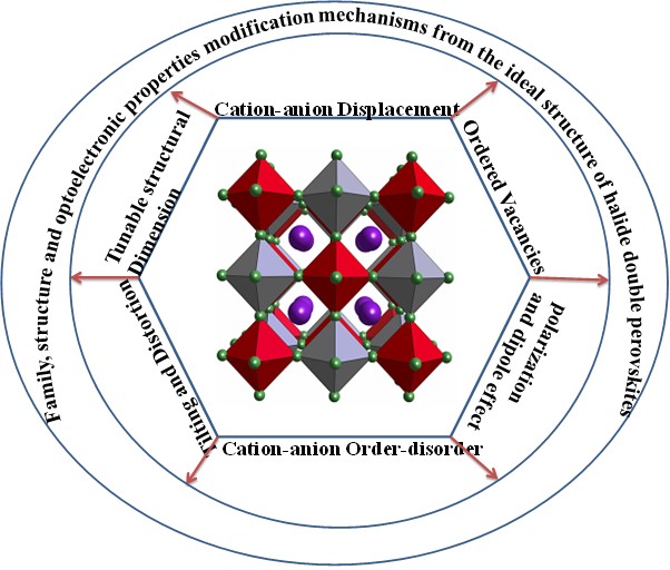
The stability issues in the widely known CH3NH3PbI3, lead to the development of alternative halide double perovskite materials, which has received great attention in recent times. Although the stability issue of double halide perovskite seems promising, their device performance remains far inferior to CH3NH3PbI3 and with challenges for further improvements. Furthermore, the power conversion efficiency of single junction organic-inorganic halide perovskite is now 24.2% and 29.15% for the textured monolithic perovskite/silicon tandem solar cell; however, for the all-inorganic halide perovskite solar cell, it is 7.11%, and halide double perovskite solar cells are based on A2BⅠBⅢX6 (A = monocation, B = cation or vacancy, X = halide) such as Cs2AgBiBr6, Cs2TiBr6, Cs2AgTlBr6 and Cs2Ag(Bi1−xInx)Br6, being 2.8% and 3.3%, respectively. This creates big questions and concerns about the performance improvement of A2BⅠBⅢX6-based perovskite solar cells. Not only is this a concern, but there are many other big challenges faced by halide double perovskite solar cells. Such big challenges include: (a) geometric constraints and limited integration with interfacial materials; (b) dynamic disorder, a wide band gap, and a localized conduction band caused by a cubic unit cell that restrains the interactions of orbitals; (c) high processing temperature which may limit the diverse applications; and (d) low electronic dimensionality that makes them less appropriate for single junction solar cell purpose, etc. Moreover, the origin of electronic and optical properties such as the polarizability, the presence of molecular dipoles, and their influence on the dynamics of the photo-excitations remain bottleneck concerns that need to be elucidated. We roadmap performance sustainable improvement, which is suggested with a particular focus on engineering material surface and bulk, band gap, interfacial, composition, doping, device architectural, polar, and domain order. The reason that this review was developed was to forward great contributions to the readers and commercial ventures.
Citation: Etsana Kiros Ashebir, Berhe Tadese Abay, Taame Abraha Berhe. Sustainable A2BⅠBⅢX6 based lead free perovskite solar cells: The challenges and research roadmap for power conversion efficiency improvement[J]. AIMS Materials Science, 2024, 11(4): 712-759. doi: 10.3934/matersci.2024036
The stability issues in the widely known CH3NH3PbI3, lead to the development of alternative halide double perovskite materials, which has received great attention in recent times. Although the stability issue of double halide perovskite seems promising, their device performance remains far inferior to CH3NH3PbI3 and with challenges for further improvements. Furthermore, the power conversion efficiency of single junction organic-inorganic halide perovskite is now 24.2% and 29.15% for the textured monolithic perovskite/silicon tandem solar cell; however, for the all-inorganic halide perovskite solar cell, it is 7.11%, and halide double perovskite solar cells are based on A2BⅠBⅢX6 (A = monocation, B = cation or vacancy, X = halide) such as Cs2AgBiBr6, Cs2TiBr6, Cs2AgTlBr6 and Cs2Ag(Bi1−xInx)Br6, being 2.8% and 3.3%, respectively. This creates big questions and concerns about the performance improvement of A2BⅠBⅢX6-based perovskite solar cells. Not only is this a concern, but there are many other big challenges faced by halide double perovskite solar cells. Such big challenges include: (a) geometric constraints and limited integration with interfacial materials; (b) dynamic disorder, a wide band gap, and a localized conduction band caused by a cubic unit cell that restrains the interactions of orbitals; (c) high processing temperature which may limit the diverse applications; and (d) low electronic dimensionality that makes them less appropriate for single junction solar cell purpose, etc. Moreover, the origin of electronic and optical properties such as the polarizability, the presence of molecular dipoles, and their influence on the dynamics of the photo-excitations remain bottleneck concerns that need to be elucidated. We roadmap performance sustainable improvement, which is suggested with a particular focus on engineering material surface and bulk, band gap, interfacial, composition, doping, device architectural, polar, and domain order. The reason that this review was developed was to forward great contributions to the readers and commercial ventures.

| [1] |
Xing GH, Mathews N, Lim SS, et al. (2014) Low-temperature solution-processed wavelength-tunable perovskites for lasing. Nature Mater 13: 476–480. https://doi.org/10.1038/nmat3911 doi: 10.1038/nmat3911

|
| [2] |
Tan ZK, Moghaddam RS, Lai ML, et al. (2014) Bright light-emitting diodes based on organometal halide perovskite. Nature Nanotech 9: 687–692. https://doi.org/10.1038/nnano.2014.149 doi: 10.1038/nnano.2014.149
|
| [3] |
Chin XY, Cortecchia D, Yin J, et al. (2015) Lead iodide perovskite light-emitting field-effect transistor. Nat Commun 6: 7383. https://doi.org/10.1038/ncomms8383 doi: 10.1038/ncomms8383
|
| [4] |
Boix PP, Nonomura K, Mathews N, et al. (2014) Current progress and future perspectives for organic/inorganic perovskite solar cells. Mater Today 17: 16–23. https://doi.org/10.1016/j.mattod.2013.12.002 doi: 10.1016/j.mattod.2013.12.002
|
| [5] |
Zhao XG, Yang DW, Ren JC, et al. (2018) Rational design of halide double perovskites for optoelectronic applications. Joule 2: 1662–1673. https://doi.org/10.1016/j.joule.2018.06.017 doi: 10.1016/j.joule.2018.06.017
|
| [6] | Li ZZ, Yin WJ (2018) Recent progress in Pb-free stable inorganic double halide perovskites. J Semicond 39: 071003. https://dx.doi.org/10.1088/1674-4926/39/7/071003 |
| [7] |
Kumar MH, Dharani S, Leong WL, et al. (2014) Lead-free halide perovskite solar cells with high photocurrents realized through vacancy modulation. Adv Mater 26: 7122–7127. https://doi.org/10.1002/adma.201401991 doi: 10.1002/adma.201401991
|
| [8] |
Hao F, Stoumpos CC, Cao DH, et al. (2014) Lead-free solid-state organic–inorganic halide perovskite solar cells. Nat Photon 8: 489–494. https://doi.org/10.1038/nphoton.2014.82 doi: 10.1038/nphoton.2014.82
|
| [9] |
Harikesh PC, Mulmudi HK, Ghosh B, et al. (2016) Rb as an alternative cation for templating inorganic lead-free perovskites for solution processed photovoltaics. Chem Mater 28: 7496–7504. https://doi.org/10.1021/acs.chemmater.6b03310 doi: 10.1021/acs.chemmater.6b03310
|
| [10] |
Linaburg ETM, Matthew R, Majher Jackson D, et al. (2017) Cs1-xRbxPbCl3 and Cs1-xRbxPbBr3 solid solutions: Understanding octahedral tilting in lead halide perovskites. Chem Mater 29: 3507-3514. https://doi.org/10.1021/acs.chemmater.6b05372 doi: 10.1021/acs.chemmater.6b05372
|
| [11] |
Volonakis G, Haghighirad AA, Milot RL (2017) Cs2InAgCl6: A new lead-free halide double perovskite with direct band gap. J Phys Chem Lett 8: 772–778. https://doi.org/10.1021/acs.jpclett.6b02682 doi: 10.1021/acs.jpclett.6b02682
|
| [12] |
Zhao XG, Yang DW, Sun YH, et al. (2017) Cu-In halide perovskite solar absorbers. J Am Chem Soc 139: 6718–6725. https://doi.org/10.1021/jacs.7b02120 doi: 10.1021/jacs.7b02120
|
| [13] |
Ju MG, Chen M, Zhou YY, et al. (2018) Earth-abundant nontoxic titanium (Ⅳ)-based vacancy-ordered double perovskite halides with tunable 1.0 to 1.8 eV bandgaps for photovoltaic applications. ACS Energy Lett 3: 297-304. https://doi.org/10.1021/acsenergylett.7b01167 doi: 10.1021/acsenergylett.7b01167
|
| [14] |
Pazoki M, Johansson MB, Zhu HM, et al. (2016) Bismuth iodide perovskite materials for solar cell applications: Electronic structure, optical transitions, and directional charge transport. J Phys Chem C 120: 29039-29046. https://doi.org/10.1021/acs.jpcc.6b11745 doi: 10.1021/acs.jpcc.6b11745
|
| [15] |
Hutter EM, Gelvez-Rueda MC, Bartesaghi D, et al. (2018) Band-like charge transport in Cs2AgBiBr6 and mixed antimony-bismuth Cs2AgBi1-xSbxBr6 halide double perovskites. ACS Omega 3: 11655-11662. https://doi.org/10.1021/acsomega.8b01705 doi: 10.1021/acsomega.8b01705
|
| [16] |
Gray MB, McClure ET, Woodward PM (2019) Cs2AgBiBr6-xClx solid solutions–band gap engineering with halide double perovskites. J Mater Chem C 7: 9686-9689. https://doi.org/10.1039/C9TC02674F doi: 10.1039/C9TC02674F
|
| [17] |
Hong KH, Kim J, Debbichi L, et al. (2017) Band gap engineering of Cs3Bi2I9 perovskites with trivalent atoms using a dual metal cation. J Phys Chem C 121: 969-974. https://doi.org/10.1021/acs.jpcc.6b12426 doi: 10.1021/acs.jpcc.6b12426
|
| [18] | Karmakar A, Dodd MS, Agnihotri S, et al. (2018) Cu(Ⅱ)-doped Cs2SbAgCl6 double perovskite: A lead-free, low-bandgap material. Chem Mater 30: 8280-8290. https://doi.org/10.1021/acs.chemmater.8b03755 |
| [19] |
Zhou J, Xia Z, Molokeev MS, et al. (2017) Composition design, optical gap and stability investigations of lead-free halide double perovskite Cs2AgInCl6. J Mater Chem A 5: 15031-15037. https://doi.org/10.1039/C7TA04690A doi: 10.1039/C7TA04690A
|
| [20] |
Chu L, Ahmad W, Liu W, et al (2019) Lead-free halide double perovskite materials: A new superstar toward green and stable optoelectronic applications. Nanomicro Lett 11: 16. https://doi.org/10.1007/s40820-019-0244-6 doi: 10.1007/s40820-019-0244-6
|
| [21] |
Tang Y, Liang M, Chang B, et al. (2019) Lead-free double halide perovskite Cs3BiBr6 with well-defined crystal structure and high thermal stability for optoelectronics. J Mater Chem C 7: 3369-3374. https://doi.org/10.1039/C8TC05480K doi: 10.1039/C8TC05480K
|
| [22] |
Luo J, Wang X, Li S, et al. (2018) Efficient and stable emission of warm-white light from lead-free halide double perovskites. Nature 563: 541-545. https://doi.org/10.1038/s41586-018-0691-0 doi: 10.1038/s41586-018-0691-0
|
| [23] |
Filip MR, Liu X, Miglio A, et al. (2018) Phase diagrams and stability of lead-free halide double perovskites Cs2BB'X6: B = Sb and Bi, B' = Cu, Ag, and Au, and X = Cl, Br, and I. J Phys Chem C 122: 158-170. https://doi.org/10.1021/acs.jpcc.7b10370 doi: 10.1021/acs.jpcc.7b10370
|
| [24] |
Flerova IN, Goreva MV, Aleksandrova KS, et al. (1998) Phase transitions in elpasolites (ordered perovskites). Mater Sci Eng R 24: 81-151. https://doi.org/10.1016/S0927-796X(98)00015-1 doi: 10.1016/S0927-796X(98)00015-1
|
| [25] |
Morss LR, Siegal M, Stenger L, et al. (1970) Preparation of cubic chloro complex compounds of trivalent metals: Cs2NaMCl6. Inorg Chem 9: 1771-1775. https://doi.org/10.1021/ic50089a034 doi: 10.1021/ic50089a034
|
| [26] |
Khalfin S, Bekenstein Y (2019) Advances in lead-free double perovskite nanocrystals, engineering band-gaps and enhancing stability through composition tunabilty. Nanoscale 11: 8665-8679. https://doi.org/10.1039/C9NR01031A doi: 10.1039/C9NR01031A
|
| [27] |
Igbari F, Wang ZK, Liao LS (2019) Progress of lead-free halide double perovskites. Adv Energy Mater 9: 1803150. https://doi.org/10.1002/aenm.201803150 doi: 10.1002/aenm.201803150
|
| [28] |
Meyer E, Mutukwa D, Zingwe N, et al. (2018) Lead-free halide double perovskites: A review of the structural, optical, and stability properties as well as their viability to replace lead halide perovskites. Metals 8: 667. https://doi.org/10.3390/met8090667 doi: 10.3390/met8090667
|
| [29] |
Slavney AH, Leppert L, Valdes AS, et al. (2018) Small-bandgap halide double perovskites. Angew Chem Int Ed 57: 12765 https://doi.org/10.1002/anie.201807421 doi: 10.1002/anie.201807421
|
| [30] | NREL Efficiency Chart. This Plot Is Courtesy of the National Renewable Energy Laboratory, Golden, CO. Available from: https://www.nrel.gov/pv/assets/pdfs/best-reserch-cell-efficiencies..20190411.pdf (accessed on 14 April 2019). |
| [31] |
Chen B, Yu Z, Liu K, et al. (2019) Grain engineering for perovskite/silicon monolithic tandem solar cells with efficiency of 25.4%. Joule 3: 177-190. https://doi.org/10.1016/j.joule.2018.10.003 doi: 10.1016/j.joule.2018.10.003
|
| [32] |
Al-Ashouri A, Köhnen E, Li B, et al. (2020) Monolithic perovskite/silicon tandem solar cell with 29% efficiency by enhanced hole extraction. Science 370: 1300-1309. https://doi.org/10.1126/science.abd401 doi: 10.1126/science.abd401
|
| [33] |
Chen M, Ju MG, Garces HF, et al. (2019) Highly stable and efficient all-inorganic lead-free perovskite solar cells with native-oxide passivation. Nat Commun 10: 16. https://doi.org/10.1038/s41467-018-07951-y doi: 10.1038/s41467-018-07951-y
|
| [34] |
Nalianya MA, Awino C, Barasa H, et al. (2021) Numerical study of lead free CsSn0.5Ge0.5I3 perovskite solar cell by SCAPS-1D. Optik 248: 168060. https://doi.org/10.1016/j.ijleo.2021.168060 doi: 10.1016/j.ijleo.2021.168060
|
| [35] |
Liu X, Li T, Hao L, et al. (2023) Lead free CsSn0.5Ge0.5I3 perovskite solar cell with different layer properties via SCAPS-1D simulation. CJCE 101: 6792-6806. https://doi.org/10.1002/cjce.25009 doi: 10.1002/cjce.25009
|
| [36] |
Singh NK, Agarwal A (2023) Performance assessment of sustainable highly efficient CsSn0.5Ge0.5I3/FASnI3 based perovskite solar cell: A numerical modelling approach. Opt Mater 139: 113822. https://doi.org/10.1016/j.optmat.2023.113822 doi: 10.1016/j.optmat.2023.113822
|
| [37] |
Aktas E, Rajamanickam N, Pascual J, et al. (2022) Challenges and strategies toward long-term stability of lead-free tin-based perovskite solar cells. Commun Mater 3: 104. https://doi.org/10.1038/s43246-022-00327-2 doi: 10.1038/s43246-022-00327-2
|
| [38] |
Saparov B, Sun JP, Meng W, et al. (2016) Thin film deposition and characterization of a Sn-deficient perovskite derivative Cs2SnI6. Chem Mater 28: 2315–2322. https://doi.org/10.1021/acs.chemmater.6b00433 doi: 10.1021/acs.chemmater.6b00433
|
| [39] |
López-Fernández I, Valli D, Wang CY, et al. (2024) Lead-free halide perovskite materials and optoelectronic devices: Progress and prospective. Adv Funct Mater 34: 2307896. https://doi.org/10.1002/adfm.202307896 doi: 10.1002/adfm.202307896
|
| [40] |
Greul E, Petrus ML, Binek A, et al. (2017) Highly stable, phase pure Cs2AgBiBr6 double perovskite thin films for optoelectronic applications. J Mater Chem A 5: 19972–19981. https://doi.org/10.1039/C7TA06816F doi: 10.1039/C7TA06816F
|
| [41] |
Yang X, Chen Y, Liu P, et al. (2020) Simultaneous power conversion efficiency and stability enhancement of Cs2AgBiBr6 lead-free inorganic perovskite solar cell through adopting a multifunctional dye interlayer. Adv Funct Mater 30: 2001557. https://doi.org/10.1002/adfm.202001557 doi: 10.1002/adfm.202001557
|
| [42] |
Zhang Z, Sun Q, Lu Y, et al. (2022) Hydrogenated Cs2AgBiBr6 for significantly improved efficiency of lead-free inorganic double perovskite solar cell. Nat Commun 13: 3397. https://doi.org/10.1038/s41467-022-31016-w doi: 10.1038/s41467-022-31016-w
|
| [43] |
Chen M, Ju MG, Carl AD, et al. (2018) Cesium titanium(IV) bromide thin films based stable lead-free perovskite solar cells. Joule 2: 1–13. https://doi.org/10.1016/j.joule.2018.01.009 doi: 10.1016/j.joule.2018.01.009
|
| [44] |
Ahmed S, Jannat F, Khan MAK, et al. (2021) Numerical development of eco-friendly Cs2TiBr6 based perovskite solar cell with all-inorganic charge transport materials via SCAPS-1D. Optik 225: 165765. https://doi.org/10.1016/j.ijleo.2020.165765 doi: 10.1016/j.ijleo.2020.165765
|
| [45] |
Mercy PAM, Wilson KSJ (2023) Development of environmental friendly high performance Cs2TiBr6 based perovskite solar cell using numerical simulation. Appl Surf Sci Adv 15: 100394. https://doi.org/10.1016/j.apsadv.2023.100394 doi: 10.1016/j.apsadv.2023.100394
|
| [46] |
Zhang P, Yang J, Wei SH (2018) Manipulation of cation combinations and configurations of halide double perovskites for solar cell absorbers. J Mater Chem A 6: 1809–1815. https://doi.org/10.1039/C7TA09713A doi: 10.1039/C7TA09713A
|
| [47] |
Berhe TA, Su WN, Chen CH, et al. (2016) Organometal halide perovskite solar cells: Degradation and stability. Energy Environ Sci 9: 323–356. https://doi.org/10.1039/C5EE02733K doi: 10.1039/C5EE02733K
|
| [48] |
Dai X, Deng Y, Van BCH, et al. (2019) Meniscus fabrication of halide perovskite thin films at high throughput for large area and low-cost solar panels. IJEM 1: 022004. https://doi.org/10.1088/2631-7990/ab263e doi: 10.1088/2631-7990/ab263e
|
| [49] |
Tiing TV (2018) Octadecylamine-functionalized single-walled carbon nanotubes for facilitating the formation of a monolithic perovskite layer and stable solar cells. Adv Funct Mater 28: 1705545. https://doi.org/10.1002/adfm.201705545 doi: 10.1002/adfm.201705545
|
| [50] |
Wu S, Liu Y (2023) Recent advancements and manipulation strategies of colloidal Cs2BIBⅢX6 lead-free halide double perovskite nanocrystals. Nano Res 16: 5572–5591. https://doi.org/10.1007/s12274-022-5232-3 doi: 10.1007/s12274-022-5232-3
|
| [51] |
Volonakis GF, Haghighirad MR, Sakai AA, et al. (2016) Lead-free halide double perovskites via heterovalent substitution of noble metals. J Phys Chem Lett 7: 1254-1259. https://doi.org/10.1021/acs.jpclett.6b00376 doi: 10.1021/acs.jpclett.6b00376
|
| [52] |
Roknuzzaman M, Zhang C, Ostrikov K, et al. (2019) Electronic and optical properties of lead-free hybrid double perovskites for photovoltaic and optoelectronic applications. Sci Rep 9: 718. https://doi.org/10.1038/s41598-018-37132-2 doi: 10.1038/s41598-018-37132-2
|
| [53] |
Stoumpos CC, Malliakas CD, Kanatzidis MG, et al. (2013) Semiconducting tin and lead iodide perovskites with organic cations: Phase transitions, high mobilities and near-infrared photoluminescent properties. Inorg Chem 52: 9019–9038. https://doi.org/10.1021/ic401215x doi: 10.1021/ic401215x
|
| [54] |
Ponseca CS, Savenije TJ, Abdellah M, et al. (2014) Organometal halide perovskite solar cell materials rationalized: Ultrafast charge generation, high and microsecond-long balanced mobilities, and slow recombination. J Am Chem Soc 136: 5189–5192. https://doi.org/10.1021/ja412583t doi: 10.1021/ja412583t
|
| [55] |
Pham HQ, Holmes RJ, Aydil ES, et al. (2019) Lead-free double perovskites Cs2InCuCl6 and (CH3NH3)2InCuCl6: Electronic, optical and electrical properties. Nanoscale 11: 11173–11182. https://doi.org/10.1039/C9NR01645G doi: 10.1039/C9NR01645G
|
| [56] |
Wei F, Deng Z, Sun S (2017) Synthesis and properties of a lead-free hybrid double perovskite: (CH3NH3)2AgBiBr6. Chem Mater 29: 1089–1094. https://doi.org/10.1021/acs.chemmater.6b03944 doi: 10.1021/acs.chemmater.6b03944
|
| [57] |
Xing G, Mathews N, Sun S, et al. (2013) Long-range balanced electron- and hole-transport lengths in organic-inorganic CH3NH3PbI3. Science 342: 344–347. https://doi.org/10.1126/science.124316 doi: 10.1126/science.124316
|
| [58] |
Etgar L, Gao P, Xue Z, et al. (2012) Mesoscopic CH3NH3PbI3/TiO2 heterojunction solar cells. J Am Chem Soc 134: 17396–17399. https://doi.org/10.1021/ja307789s doi: 10.1021/ja307789s
|
| [59] |
Ball JM, Lee MM, Hey A, et al. (2013) Low-temperature processed meso-superstructured to thin-film perovskite solar cells. Energy Environ Sci 6: 1739–1743. https://doi.org/10.1039/C3EE40810H doi: 10.1039/C3EE40810H
|
| [60] |
Jeon NJ, Noh JH, Kim YC, et al. (2014) Solvent engineering for high-performance inorganic–organic hybrid perovskite solar cells. Nat Mater 13: 897–903. https://doi.org/10.1038/nmat4014 doi: 10.1038/nmat4014
|
| [61] |
Burschka J, Pellet N, Moon SJ, et al. (2013) Sequential deposition as a route to high-performance perovskite-sensitized solar cells. Nature 499: 316–319. https://doi.org/10.1038/nature12340 doi: 10.1038/nature12340
|
| [62] |
Liu D, Kelly TL (2014) Perovskite solar cells with a planar heterojunction structure prepared using room-temperature solution processing techniques. Nat Photon 8: 133–138. https://doi.org/10.1038/nphoton.2013.342 doi: 10.1038/nphoton.2013.342
|
| [63] |
Eperon GE, Stranks SD, Menelaou C (2014) Formamidinium lead trihalide: A broadly tunable perovskite for efficient planar heterojunction solar cells. Energy Environ Sci 7: 982–988. https://doi.org/10.1039/C3EE43822H doi: 10.1039/C3EE43822H
|
| [64] |
Kojima A, Teshima K, Shirai Y, et al. (2009) Organometal halide perovskites as visible-light sensitizers for photovoltaic cells. J Am Chem Soc 131: 6050–6051. https://doi.org/10.1021/ja809598r doi: 10.1021/ja809598r
|
| [65] |
Ghanshyam PVB, Kim C, Lookman T (2016) Finding new perovskite halides via machine learning. Front Mater 3: 19. https://doi.org/10.3389/fmats.2016.00019 doi: 10.3389/fmats.2016.00019
|
| [66] |
Gonzalez-Pedro V, Juarez-Perez EJ, Arsyad WS (2014) General working principles of CH3NH3PbX3 perovskite solar cells. Nano Lett 14: 888–893. https://doi.org/10.1021/nl404252e doi: 10.1021/nl404252e
|
| [67] |
Uddin MA, Calabro RL, Kim DY, et al. (2018) Halide exchange and surface modification of metal halide perovskite nanocrystals with alkyltrichlorosilanes. Nanoscale 10: 16919–16927. https://doi.org/10.1039/C8NR04763D doi: 10.1039/C8NR04763D
|
| [68] |
Protesescu L, Yakunin S, Bodnarchuk MI (2015) Nanocrystals of cesium lead halide perovskites (CsPbX3, X = Cl, Br, and I): Novel optoelectronic materials showing bright emission with wide color gamut. Nano Lett 15: 3692–3696. https://doi.org/10.1021/nl5048779 doi: 10.1021/nl5048779
|
| [69] |
Nedelcu G, Protesescu L, Yakunin S (2015) Fast anion-exchange in highly luminescent nanocrystals of cesium lead halide perovskites (CsPbX3, X = Cl, Br, I). Nano Lett 15: 5635–5640. https://doi.org/10.1021/acs.nanolett.5b02404 doi: 10.1021/acs.nanolett.5b02404
|
| [70] |
Jeon JHN, Yang WS, Kim YC, et al. (2015) Compositional engineering of perovskite materials for high-performance solar cells. Nature 517: 476–480. https://doi.org/10.1038/nature14133 doi: 10.1038/nature14133
|
| [71] |
Lee JW, Kim DH, Kim KS, et al. (2015) Formamidinium and cesium hybridization for photo- and moisture-stable perovskite solar cell. Adv Energy Mater 5: 1501310. https://doi.org/10.1002/aenm.201501310 doi: 10.1002/aenm.201501310
|
| [72] |
Park YH, Jeong I, Bae S, et al. (2017) Inorganic rubidium cation as an enhancer for photovoltaic performance and moisture stability of HC(NH2)2PbI3 perovskite solar cells. Adv Funct Mater 27: 1605988. https://doi.org/10.1002/adfm.201605988 doi: 10.1002/adfm.201605988
|
| [73] |
Locardi F, Cirignano M, Dmitry BZD, et al. (2018) Colloidal synthesis of double perovskite Cs2AgInCl6 and Mn-doped Cs2AgInCl6 nanocrystals. J Am Chem Soc 140: 12989–12995 https://doi.org/10.1021/jacs.8b07983 doi: 10.1021/jacs.8b07983
|
| [74] |
Stoumpos CCF, Clark L, Kim DJ, et al. (2015) Hybrid germanium iodide perovskite semiconductors: Active lone pairs, structural distortions, direct and indirect energy gaps, and strong nonlinear optical properties. J Am Chem Soc 137: 6804-6819. https://doi.org/10.1021/jacs.5b01025 doi: 10.1021/jacs.5b01025
|
| [75] |
Berhe TA, Su WN, Hwang BJ (2024) Halide perovskites' multifunctional properties: Coordination engineering, coordination chemistry, electronic interactions and energy applications beyond photovoltaics. Inorganics 12: 182. https://doi.org/10.3390/inorganics12070182 doi: 10.3390/inorganics12070182
|
| [76] |
Hua WAE, Johansson MB, Wang J, (2021) Mixed-halide double perovskite Cs2AgBiX6 (X = Br, I) with tunable optical properties via anion exchange. ChemSusChem 14: 4507–4515. https://doi.org/10.1002/cssc.202101146 doi: 10.1002/cssc.202101146
|
| [77] |
Abdulmutta T, Rassamessan A (2024) First-principles study on structural, electronic and optical properties of mixed alloys of Cs2Ag(SbxBi). Comput Mater Sci 239. https://doi.org/10.1039/D3RA02566G doi: 10.1039/D3RA02566G
|
| [78] |
Noel NK, Stranks SD, Abate A, et al. (2014). Lead-free organic–inorganic tin halide perovskites for photovoltaic applications. Energy Environ Sci 7: 3061–3068. https://doi.org/10.1039/C4EE01076K doi: 10.1039/C4EE01076K
|
| [79] |
Xiao ZY, Shao Y, Wang Y, et al. (2015) Giant switchable photovoltaic effect in organometal trihalide perovskite devices. Nat Mater 14: 193-198. https://doi.org/10.1038/nmat4150 doi: 10.1038/nmat4150
|
| [80] |
Bertoluzzi LS, Liu RS, Lee L, et.al. (2015) Cooperative kinetics of depolarization in CH3NH3PbI3 perovskite solar cells. Energy Environ Sci 8: 910–915. https://doi.org/10.1039/C4EE03171G doi: 10.1039/C4EE03171G
|
| [81] |
Snaith HJA, Ball A, Eperon JM, et al. (2014) Anomalous hysteresis in perovskite solar cells. J Phys Chem Lett 5: 1511–1515. https://doi.org/10.1021/jz500113x doi: 10.1021/jz500113x
|
| [82] |
Tress WM, Moehl N, Zakeeruddin T, et al. (2015) Understanding the rate-dependent J-V hysteresis, slow time component, and aging in CH3NH3PBI3 perovskite solar cells: The role of a compensated electric field. Energy Environ Sci 8: 995–1004. https://doi.org/10.1039/C4EE03664F doi: 10.1039/C4EE03664F
|
| [83] |
Hoke ET, Slotcavage DJ, Dohner ER, et al. (2015) Reversible photo-induced trap formation in mixed-halide hybrid perovskites for photovoltaics. Chem Sci 6: 613–617. https://doi.org/10.1039/C4SC03141E doi: 10.1039/C4SC03141E
|
| [84] |
Fan ZX, Sun J, Chen K, et al. (2015) Ferroelectricity of CH3NH3PbI3 perovskite. J Phys Chem Lett 6: 1155–1161. https://doi.org/10.1021/acs.jpclett.5b00389 doi: 10.1021/acs.jpclett.5b00389
|
| [85] |
Rong Y, Hu Y, Ravishankar S, et al. (2017) Tunable hysteresis effect for perovskite solar cells, Energy Environ Sci 10: 2383–2391. https://doi.org/10.1039/C7EE02048A doi: 10.1039/C7EE02048A
|
| [86] |
Balaguera EH, Bisquert J (2024) Accelerating the assessment of hysteresis in perovskite solar cells. ACS Energy Lett 9: 478–486. https://doi.org/10.1021/acsenergylett.3c02779 doi: 10.1021/acsenergylett.3c02779
|
| [87] | Singh R, Parashar M (2020) Origin of hysteresis in perovskite solar cells, In: Ren JZ, Kan ZP, Soft-Matter Thin Film Solar Cells: Physical Processes and Device Simulation, New York: AIP Publishing LLC. https://doi.org/10.1063/9780735422414_001 |
| [88] |
Kim HS, Park NG (2014) Parameters affecting Ⅰ–Ⅴ hysteresis of CH3NH3PbI3 perovskite solar cells: Effects of perovskite crystal size and mesoporous TiO2 layer. J Phys Chem Lett 5: 2927–2934. https://doi.org/10.1021/jz501392m doi: 10.1021/jz501392m
|
| [89] |
Leijtens T, Ram SKA, Eperon GE, et al. (2015) Modulating the electron-hole interaction in a hybrid lead halide perovskite with an electric field. J Am Chem Soc 137: 15451–15459. https://doi.org/10.1021/jacs.5b09085 doi: 10.1021/jacs.5b09085
|
| [90] |
Chaves A, Azadani JG, Alsalman H, et al. (2020) Low bandgap engineering of two-dimensional semiconductor materials. npj 2D Mater Appl 4: 29. https://doi.org/10.1038/s41699-020-00162-4 doi: 10.1038/s41699-020-00162-4
|
| [91] |
Prasanna R, Gold-Parker A, Leijtens T, et al. (2017) Band gap tuning via lattice contraction and octahedral tilting in perovskite materials for photovoltaics. J Am Chem Soc 139: 11117–11124. https://doi.org/10.1021/jacs.7b04981 doi: 10.1021/jacs.7b04981
|
| [92] |
Lee JH, Bristowe NC, Lee JH, et al. (2016) Resolving the physical origin of octahedral tilting in halide perovskites. Chem Mater 28: 4259–4266. https://doi.org/10.1021/acs.chemmater.6b00968 doi: 10.1021/acs.chemmater.6b00968
|
| [93] |
Bechtel JS, Van der Ven A (2018) Octahedral tilting instabilities in inorganic halide perovskites. Phys Rev Materials 2: 025401. https://doi.org/10.1103/PhysRevMaterials.2.025401 doi: 10.1103/PhysRevMaterials.2.025401
|
| [94] |
Yang RX, Skelton JM, Silva EL, et al. (2017) Spontaneous octahedral tilting in the cubic inorganic cesium halide perovskites CsSnX3 and CsPbX3 (X = F, Cl, Br, I). J Phys Chem Lett 8: 4720-4726. https://doi.org/10.1021/acs.jpclett.7b02423 doi: 10.1021/acs.jpclett.7b02423
|
| [95] |
Shao Y, Gao W, Yan H, (2022) Unlocking surface octahedral tilt in twodimensional Ruddlesden-Popper perovskites. Nat Commun 13: 138. https://doi.org/10.1038/s41467-021-27747-x doi: 10.1038/s41467-021-27747-x
|
| [96] |
Klarbring J (2018) Low energy paths for octahedral tilting in inorganic halide perovskites. Phys Rev B 99: 104105. https://doi.org/10.1103/PhysRevB.99.104105 doi: 10.1103/PhysRevB.99.104105
|
| [97] |
Munson KT, Kennehan ER, Doucette GS, et al. (2018) Dynamic disorder dominates delocalization, transport, and recombination in halide perovskites. Chem 4: 2826-2843. https://doi.org/10.1016/j.chempr.2018.09.00199 doi: 10.1016/j.chempr.2018.09.00199
|
| [98] |
Lei H, Hardy D, Gao F (2021) Lead‐free double perovskite Cs2AgBiBr6: Fundamentals, applications and perspectives. Adv Funct Mater 31: 2105898. https://doi.org/10.1002/adfm.202105898 doi: 10.1002/adfm.202105898
|
| [99] | Karunadasa HI, Slavney AH (2022) Alloyed halide double perovskites as solar-cell absorbers. Available from: https://www.osti.gov/servlets/purl/1892693. |
| [100] |
Palmstrom AF, Eperon GE, Leijtens T, et al. (2019) Enabling flexible all-perovskite tandem solar cells. Joule 3: 1–12. https://doi.org/10.1016/j.joule.2019.05.009 doi: 10.1016/j.joule.2019.05.009
|
| [101] |
Zhou L, Xu YF, Chen BX, et al. (2018) Synthesis and photocatalytic application of stable lead free Cs2AgBiBr6 perovskite nanocrystals. Small 14: 1703762. https://doi.org/10.1002/smll.201703762 doi: 10.1002/smll.201703762
|
| [102] |
Zhang ZZ, Liang Y, Huang H, et al. (2019) Stable and highly efficient photocatalysis with lead-free double-perovskite of Cs2AgBiBr6. Angew Chem Int Ed 58: 7263–7267. https://doi.org/10.1002/anie.201900658 doi: 10.1002/anie.201900658
|
| [103] |
Cho J, DuBose JT, Kamat PV (2020) Charge injection from excited Cs2AgBiBr6 quantum dots into semiconductor oxides. Chem Mater 32: 510–517. https://doi.org/10.1021/acs.chemmater.9b04243 doi: 10.1021/acs.chemmater.9b04243
|
| [104] |
Ippili S, Kim JH, Jella V, et al. (2023) Halide double perovskite-based efficient mechanical energy harvester and storage devices for self-charging power unit. Nano Energy 107: 108148. https://doi.org/10.1016/j.nanoen.2022.108148 doi: 10.1016/j.nanoen.2022.108148
|
| [105] |
Wu H, Pi J, Liu Q, et al. (2021) All-inorganic lead free double perovskite li-battery anode material hosting high Li+ ion concentrations. J Phys Chem Lett 12: 4125–4129. https://doi.org/10.1021/acs.jpclett.1c00041 doi: 10.1021/acs.jpclett.1c00041
|
| [106] |
Zhang L, Miao J, Li J, et al. (2020) Halide perovskite materials for energy storage applications. Adv Funct Mater 30: 2003653. https://doi.org/10.1002/adfm.202003653 doi: 10.1002/adfm.202003653
|
| [107] |
Yang S, Liang Q, Wu H, et al. (2022) Lead-free double perovskite Cs2NaErCl6: Li+ as high-stability anodes for Li-ion batteries. J Phys Chem Lett 13: 4981–4987. https://doi.org/10.1021/acs.jpclett.2c01052 doi: 10.1021/acs.jpclett.2c01052
|
| [108] |
Choon SL, Lim HN (2024) Impact of vacancies in halide perovskites for batteries and supercapacitors. Mater Today Energy 43: 101577. https://doi.org/10.1016/j.mtener.2024.101577 doi: 10.1016/j.mtener.2024.101577
|
| [109] |
Yadav A, Saini A, Kumar P, et al. (2024) Lead-free halide perovskites for high-performance thin-film flexible supercapacitor applications. J Mater Chem C 12: 197–206. https://doi.org/10.1039/D3TC02784H doi: 10.1039/D3TC02784H
|
| [110] |
Tan Y, Mu G, Chen M, et al. (2023) X-ray detectors based on halide perovskite materials. Coatings 13: 211. https://doi.org/10.3390/coatings13010211 doi: 10.3390/coatings13010211
|
| [111] |
Tailor NK, Ghosh J, Afroz MA, et al. (2022) Self-powered X-ray detection and imaging using Cs2AgBiCl6 lead-free double perovskite single crystal. ACS Appl Electron Mater 4: 4530–4539. https://doi.org/10.1021/acsaelm.2c00752 doi: 10.1021/acsaelm.2c00752
|
| [112] |
Li Z, Zhou F, Yao H, et al. (2021) Halide perovskites for high-performance X-ray detector. Materials Today 48: 155–175. https://doi.org/10.1016/j.mattod.2021.01.028 doi: 10.1016/j.mattod.2021.01.028
|
| [113] |
Saparov B, Mitzi DB (2016) Organic–inorganic perovskites: structural versatility for functional materials design. Chem Rev 116: 4558–4596. https://doi.org/10.1021/acs.chemrev.5b00715 doi: 10.1021/acs.chemrev.5b00715
|
| [114] | Best Research-Cell Efficiency Chart. (2019) Available from: https://www.nrel.gov/pv/cell-efficiency.html. |
| [115] |
Bhojak V, Bhatia D, Jain PK (2022) Investigation of photocurrent efficiency of Cs2TiBr6 double perovskite solar cell. Mater Today Proc 66: 3692–3697. https://doi.org/10.1016/j.matpr.2022.07.443 doi: 10.1016/j.matpr.2022.07.443
|
| [116] |
Qin X, Zhao Z, Wang Y, et al. (2017) Recent progress in stability of perovskite solar cells. J Semicond 38: 011002. https://doi.org/10.1088/1674-4926/38/1/011002 doi: 10.1088/1674-4926/38/1/011002
|
| [117] |
Berhe TA, Cheng JH, Su WN, et al. (2017) Identification of the physical origin behind disorder, heterogeneity, and reconstruction and their correlation with the photoluminescence lifetime in hybrid perovskite thin films. J Mater Chem A 5: 21002–21015. https://doi.org/10.1039/C7TA04615D doi: 10.1039/C7TA04615D
|
| [118] |
Xiao Z, Meng W, Wang J, et al. (2017) Searching for promising new perovskite-based photovoltaic absorbers: The importance of electronic dimensionality. Mater Horiz 4: 206–216. https://doi.org/10.1039/C6MH00519E doi: 10.1039/C6MH00519E
|
| [119] |
Zhang Q, Ting H, Wei S, et al. (2018) Recent progress in lead-free perovskite (-like) solar cells. Mater Today Energy 8: 157–165. https://doi.org/10.1016/j.mtener.2018.03.001 doi: 10.1016/j.mtener.2018.03.001
|
| [120] |
Kanno S, Imamura Y, Hada M (2019) Alternative materials for perovskite solar cells from materials informatics. Phys Rev Mater 3: 075403. https://doi.org/10.1103/PhysRevMaterials.3.075403 doi: 10.1103/PhysRevMaterials.3.075403
|
| [121] |
Liang L, Gao P (2018) Lead-free hybrid perovskite absorbers for viable application: Can we eat the cake and have it too? Adv Sci (Weinh) 5: 1700331. https://doi.org/10.1002/advs.201700331 doi: 10.1002/advs.201700331
|
| [122] |
Abate A (2017) Perovskite solar cells go lead free. Joule 1: 659–664. https://doi.org/10.1016/j.joule.2017.09.007 doi: 10.1016/j.joule.2017.09.007
|
| [123] |
Xu Q, Yang D, Lv J, et al. (2018) Perovskite solar absorbers: Materials by design. Small Methods 2: 1700316. https://doi.org/10.1002/smtd.201700316 doi: 10.1002/smtd.201700316
|
| [124] |
Volonakis G, Giustino F (2018) Surface properties of lead-free halide double perovskites: Possible visible-light photo-catalysts for water splitting featured. Appl Phys Lett 112: 243901. https://doi.org/10.1063/1.5035274 doi: 10.1063/1.5035274
|
| [125] |
Slavney AH, Hu T, Lindenberg AM, et al. (2016) A bismuth-halide double perovskite with long carrier recombination lifetime for photovoltaic applications. J Am Chem Soc 138: 2138-2141. https://doi.org/10.1021/jacs.5b13294 doi: 10.1021/jacs.5b13294
|
| [126] | Karunadasa HI, Slavney AH (2017) Halide double perovskite Cs2AgBiBr6 solar-cell absorber having long carrier lifetimes. |
| [127] |
Savory CN, Walsh A, Scanlon DO (2016) Can Pb-free halide double perovskites support high-efficiency solar cells? ACS Energy Lett 1: 949-955. https://doi.org/10.1021/acsenergylett.6b00471 doi: 10.1021/acsenergylett.6b00471
|
| [128] |
Pecunia V, Occhipinti LG, Chakraborty A (2020) Lead-free halide perovskite photovoltaics: Challenges, open questions, and opportunities. APL Materials 8: 100901. https://doi.org/10.1063/5.0022271 doi: 10.1063/5.0022271
|
| [129] |
Rühle S (2017) The detailed balance limit of perovskite/silicon and perovskite/CdTe tandem solar cells. Phys Status Solidi A 214: 1600955. https://doi.org/10.1002/pssa.201600955 doi: 10.1002/pssa.201600955
|
| [130] |
Sheng R, Ho-Baillie AWY, Huang SJ, et al. (2015) Four-terminal tandem solar cells using CH3NH3PbBr3 by spectrum splitting. J Phys Chem Lett 6: 3931-3934. https://doi.org/10.1021/acs.jpclett.5b01608 doi: 10.1021/acs.jpclett.5b01608
|
| [131] |
Sani F, Shafie S, Lim HN (2018) Advancement on lead-free organic-inorganic halide perovskite solar cells: A review. Materials 11: 1008. https://doi.org/10.3390/ma11061008 doi: 10.3390/ma11061008
|
| [132] |
Righetto M, Caicedo-Dávila S, Sirtl MT, et al. (2023) Alloying effects on charge-carrier transport in silver–bismuth double perovskites. J Phys Chem Lett 14: 10340–10347 https://doi.org/10.1021/acs.jpclett.3c02750 doi: 10.1021/acs.jpclett.3c02750
|
| [133] |
Bartesaghi D, Slavney AH, Gélvez-Rueda MC, et al. (2018) Charge carrier dynamics in Cs2AgBiBr6 double perovskite. J Phys Chem C 122: 4809–4816. https://doi.org/10.1021/acs.jpcc.8b00572 doi: 10.1021/acs.jpcc.8b00572
|
| [134] |
Joshua-Leveillee GV, Giustino F (2021) Phonon-limited mobility and electronphonon coupling in lead-free halide double perovskites. J Phys Chem Lett 12: 4474–4482. https://doi.org/10.1021/acs.jpclett.1c00841 doi: 10.1021/acs.jpclett.1c00841
|
| [135] |
Lin H, Zhou C, Tian Y (2018) Low-dimensional organometal halide perovskites. ACS Energy Lett 3: 54-62. https://doi.org/10.1021/acsenergylett.7b00926 doi: 10.1021/acsenergylett.7b00926
|
| [136] |
Han D, Shi H, Ming W, et al. (2018) Unraveling luminescence mechanisms in zero-dimensional halide perovskites. J Mater Chem C 6: 6398-6405. https://doi.org/10.1039/C8TC01291A doi: 10.1039/C8TC01291A
|
| [137] |
Duan D, Ge C, Rahaman MZ, et al. (2023) Recent progress with one-dimensional metal halide perovskites: from rational synthesis to optoelectronic applications. NPG Asia Mater 15: 8. https://doi.org/10.1038/s41427-023-00465-0 doi: 10.1038/s41427-023-00465-0
|
| [138] |
Qiu T, Hu Y, Xu F (2018) Recent advances in one-dimensional halide perovskites for optoelectronic applications. Nanoscale 10: 20963-20989. https://doi.org/10.1039/C8NR05862H doi: 10.1039/C8NR05862H
|
| [139] |
Chen X, Zhou H, Wang H (2021) 2D/3D halide perovskites for optoelectronic devices. Front Chem 9. https://doi.org/10.3389/fchem.2021.715157 doi: 10.3389/fchem.2021.715157
|
| [140] |
Fiorentino F, Albaqami MD, Poli I, et al. (2022) Thermal- and light-induced evolution of the 2D/3D interface in lead-halide perovskite films. ACS Appl Mater Interfaces 14: 34180-34188. https://doi.org/10.1021/acsami.1c09695 doi: 10.1021/acsami.1c09695
|
| [141] |
Kim EB, Akhtar MS, Shin HS, et al. (2021) A review on two-dimensional (2D) and 2D-3D multidimensional perovskite solar cells: Perovskites structures, stability, and photovoltaic performances. J Photochem Photobiol C 48: 100405. https://doi.org/10.1016/j.jphotochemrev.2021.100405 doi: 10.1016/j.jphotochemrev.2021.100405
|
| [142] |
Etgar L (2018) The merit of perovskite's dimensionality; can this replace the 3D halide perovskite? Energy Environ Sci 11: 234-242. https://doi.org/10.1039/C7EE03397D doi: 10.1039/C7EE03397D
|
| [143] |
Marongiu D, Saba M, Quochi F (2019) The role of excitons in 3D and 2D lead halide perovskites. J Mater Chem C 7: 12006-12018. https://doi.org/10.1039/C9TC04292J doi: 10.1039/C9TC04292J
|
| [144] |
Moral RF, Perini CAR, Kodalle T, et al. (2024) Anion and cation migration at 2D/3D halide perovskite interfaces. ACS Energy Lett 9: 2703-2716. https://doi.org/10.1021/acsenergylett.4c00728 doi: 10.1021/acsenergylett.4c00728
|
| [145] |
Filip MR, Hillman S, Haghighirad AA, et al. (2016) Band gaps of the lead-free halide double perovskites: Cs2BiAgCl6 and Cs2BiAgBr6 from theory and experiment. J Phys Chem Lett 7: 2579-2585. https://doi.org/10.1021/acs.jpclett.6b01041 doi: 10.1021/acs.jpclett.6b01041
|
| [146] |
McClure ETB, Windl MR, Woodward PMW (2016) Cs2AgBiX6 (X = Br, Cl): New visible light absorbing, lead-free halide perovskite semiconductors. Chem Mater 28: 1348-1354. https://doi.org/10.1021/acs.chemmater.5b04231 doi: 10.1021/acs.chemmater.5b04231
|
| [147] |
Luo SLJ, Wu H, Zhou Y, et al. (2018) Cs2AgInCl6 double perovskite single crystals: Parity forbidden transitions and their application for sensitive and fast UV photodetectors. ACS Photonics 5: 398. https://doi.org/10.1021/acsphotonics.7b00837 doi: 10.1021/acsphotonics.7b00837
|
| [148] |
Zhou HC, Li Q, Luo G, et al. (2014) Interface engineering of highly efficient perovskite solar cells. Science 345: 542-546. https://doi.org/10.1126/science.1254050 doi: 10.1126/science.1254050
|
| [149] |
De Quilettes DWV, Stranks SM, Nagaoka SD, et al. (2015) Impact of microstructure on local carrier lifetime in perovskite solar cells. Science 348: 683-686. https://doi.org/10.1126/science.aaa5333 doi: 10.1126/science.aaa5333
|
| [150] |
Rui SHH, Chen T, Gui R, et al. (2023) Extracting energetic disorder in organic solar cells using percolation models. ChemPhysMater 2: 52–57. https://doi.org/10.1016/j.chphma.2022.03.002 doi: 10.1016/j.chphma.2022.03.002
|
| [151] |
Wang DD, Li YS, Yang YG, et al. (2024) Energetic disorder dominates optical properties and recombination dynamics in tin-lead perovskite nanocrystals. eScience 100279. https://doi.org/10.1016/j.esci.2024.100279 doi: 10.1016/j.esci.2024.100279
|
| [152] |
Yang C, Ma L, Xu Y (2022) Reduced energetic disorder enables over 14% efficiency in organic solar cells based on completely non-fused-ring donors and acceptors. Sci China Chem 65: 2604–2612. https://doi.org/10.1007/s11426-022-1449-4 doi: 10.1007/s11426-022-1449-4
|
| [153] |
Diez-Cabanes V, Samuele G, Beljonne D, et al. (2023) On the origin of energetic disorder in mixed halides lead perovskites. Adv Optical Mater 12: 2301105. https://doi.org/10.1002/adom.202301105 doi: 10.1002/adom.202301105
|
| [154] |
Liu Y, Banon JP, Frohna K, et al. (2023) The electronic disorder landscape of mixed halide perovskites. ACS Energy Lett 8: 250-258. https://doi.org/10.1021/acsenergylett.2c02352 doi: 10.1021/acsenergylett.2c02352
|
| [155] |
Yin A, Zhang D, Cheung SH, et al. (2018) On the understanding of energetic disorder, charge recombination and voltage losses in all-polymer solar cells. J Mater Chem C 6: 7855–7863. https://doi.org/10.1039/C8TC02689K doi: 10.1039/C8TC02689K
|
| [156] |
Igbari F, Wang R, Wang ZK, et al. (2019) Composition stoichiometry of Cs2AgBiBr6 films for highly efficient lead-free perovskite solar cells. Nano Lett 19: 2066–2073. https://doi.org/10.1021/acs.nanolett.9b00238 doi: 10.1021/acs.nanolett.9b00238
|
| [157] |
Bush KA, Frohna K, Prasanna R, et al. (2018) Compositional engineering for efficient wide band gap perovskites with improved stability to photoinduced phase segregation. ACS Energy Lett 3: 428–435. https://doi.org/10.1021/acsenergylett.7b01255 doi: 10.1021/acsenergylett.7b01255
|
| [158] |
Yang J, Zhang P, Wei SH (2018) Band structure engineering of Cs2AgBiBr6 perovskite through order–disordered transition: A first-principle study. J Phys Chem Lett 9: 31–35. https://doi.org/10.1021/acs.jpclett.7b02992 doi: 10.1021/acs.jpclett.7b02992
|
| [159] |
Kim J, Kim H, Mahesh C, et al. (2018) Impacts of cation ordering on bandgap dispersion of double perovskites. APL Materials 6: 084903. https://doi.org/10.1063/1.5027230 doi: 10.1063/1.5027230
|
| [160] |
Liu Z, Li H, Qin C, et al. (2019) Solution-processed inorganic perovskite flexible photodetectors with high performance. Nanoscale Res Lett 14: 284. https://doi.org/10.1186/s11671-019-3120-x doi: 10.1186/s11671-019-3120-x
|
| [161] | Chilvery A, Das S, Guggilla P, et al. (2016) A perspective on the recent progress in solution-processed methods for highly efficient perovskite solar cells. STAM 17: 650–658. http://dx.doi.org/10.1080/14686996.2016.1226120 |
| [162] |
Seo JW, Noh JH, Seok SI (2016) Rational strategies for efficient perovskite solar cells. Acc Chem Res 49: 562–572. https://doi.org/10.1021/acs.accounts.5b00444 doi: 10.1021/acs.accounts.5b00444
|
| [163] |
Arain Z, Liu C, Yang Y, et al. (2019) Elucidating the dynamics of solvent engineering for perovskite solar cells. Sci China Mater 62: 161–172. https://doi.org/10.1007/s40843-018-9336-1 doi: 10.1007/s40843-018-9336-1
|
| [164] |
Li J, Yang R, Que L, et al. (2019) Optimization of anti-solvent engineering toward high performance perovskite solar cells. J Mater Res 34: 2416–2424. https://doi.org/10.1557/jmr.2019.122 doi: 10.1557/jmr.2019.122
|
| [165] |
Duan J, Xu H, Sha W, et al. (2019) Inorganic perovskite solar cells: An emerging member of the photovoltaic community. J Mater Chem A 7: 21036–21068. https://doi.org/10.1039/C9TA06674H. doi: 10.1039/C9TA06674H
|
| [166] |
Li B, Fu L, Li S, et al. (2019) Pathways toward high-performance inorganic perovskite solar cells: Challenges and strategies. J Mater Chem A 7: 20494–20518. https://doi.org/10.1039/C9TA04114A doi: 10.1039/C9TA04114A
|
| [167] |
Wang P, Zhang X, Zhou Y, et al. (2018) Solvent-controlled growth of inorganic perovskite films in dry environment for efficient and stable solar cells. Nat Commun 9: 2225. https://doi.org/10.1038/s41467-018-04636-4 doi: 10.1038/s41467-018-04636-4
|
| [168] | DeHoff RT (1999) Engineering of microstructures. Mater Res 2: 111–126. http://dx.doi.org/10.1590/S1516-14391999000300002 |
| [169] | Clemens H, Mayer S, Scheu C (2017) Microstructure and properties of engineering materials: From fundamentals to applications, In: Staron P, Schreyer A, Clemens H, Mayer S, In Neutrons and Synchrotron Radiation in Engineering Materials Science, New York: John Wiley & Sons. https://doi.org/10.1002/9783527684489.ch1 |
| [170] |
Szuromi P (1997) Microstructural engineering of materials. Science 277: 1183. https://doi.org/10.1126/science.277.5330.1183 doi: 10.1126/science.277.5330.1183
|
| [171] |
Chen L, Paillard C, Zhao HJ, et al. (2018) Tailoring properties of hybrid perovskites by domain-width engineering with charged walls. npj Computat Mater 4: 75. https://doi.org/10.1038/s41524-018-0134-3 doi: 10.1038/s41524-018-0134-3
|
| [172] |
Schade L, Wright AD, Johnson RD, et al. (2019) Structural and optical properties of Cs2AgBiBr6 double perovskite. ACS Energy Lett 4: 299–305. https://doi.org/10.1021/acsenergylett.8b02090 doi: 10.1021/acsenergylett.8b02090
|
| [173] |
Lozhkina OA, Murashkina AA, Elizarov MS, et al. (2018) Microstructural analysis and optical properties of the halide double perovskite Cs2BiAgBr6 single crystals. Chem Phys Lett 694: 18–22. https://doi.org/10.1016/j.cplett.2018.01.031 doi: 10.1016/j.cplett.2018.01.031
|
| [174] |
Liu W, Liu Y, Wang J, et al. (2018) Twin domains in organometallic halide perovskite thin-films. Crystals 8: 216. https://doi.org/10.3390/cryst8050216 doi: 10.3390/cryst8050216
|
| [175] |
Liu S, Zheng F, Koocher NZ, et al. (2015) Ferroelectric domain wall induced band gap reduction and charge separation in organometal halide perovskites. J Phys Chem Lett 6: 693-699. https://doi.org/10.1021/jz502666j doi: 10.1021/jz502666j
|
| [176] |
You L, Zheng F, Fang L, et al. (2018) Enhancing ferroelectric photovoltaic effect by polar order engineering. Sci Adv 4: eaat3438. https://doi.org/10.1126/sciadv.aat3438 doi: 10.1126/sciadv.aat3438
|
| [177] |
Li Y, Fu J, Mao X, et al. (2021) Enhanced bulk photovoltaic effect in two-dimensional ferroelectric CuInP2S6. Nat Commun 12: 5896. https://doi.org/10.1038/s41467-021-26200-3 doi: 10.1038/s41467-021-26200-3
|
| [178] |
Shockley W, Queisser HJ (1961) Detailed balance limit of efficiency of P-N junction solar cells. J Appl Phys 32: 510–511. https://doi.org/10.1063/1.1736034 doi: 10.1063/1.1736034
|
| [179] |
Ihtisham ULH, Khan MI, Ullah A, et al. (2024) Bandgap reduction and efficiency enhancement in Cs2AgBiBr6 double perovskite solar cells through gallium substitution. RSC Adv 14: 5440–5448. https://doi.org/10.1039/D3RA08965G doi: 10.1039/D3RA08965G
|
| [180] |
Du KZ, Meng W, Wang X, et al. (2017) Bandgap engineering of lead-free double perovskite Cs2AgBiBr6 through trivalent metal alloying. Angew Chem Int Ed 8158–8162. https://doi.org/10.1002/anie.201703970 doi: 10.1002/anie.201703970
|
| [181] |
Yan K, Long M, Zhang T, et al. (2015) Hybrid halide perovskite solar cell precursors: Colloidal chemistry and coordination engineering behind device processing for high efficiency. J Am Chem Soc 137: 4460–4468. https://doi.org/10.1021/jacs.5b00321 doi: 10.1021/jacs.5b00321
|
| [182] |
Bellakhdar T, Nabi Z, Bouabdallah B, et al. (2022) Ab initio study of structural, electronic, mechanical and optical properties of the tetragonal Cs2AgBiBr6 halide double perovskite. Appl Phys A 128: 155. https://doi.org/10.1007/s00339-022-05276-8 doi: 10.1007/s00339-022-05276-8
|
| [183] |
Merabet B, Alamri H, Djermouni M (2012) Optimal bandgap of double perovskite la-substituted Bi2FeCrO6 for solar cells: An ab initio GGA+U study. Chin Phys Lett 34: 016101. https://doi.org/10.1088/0256-307X/34/1/016101 doi: 10.1088/0256-307X/34/1/016101
|
| [184] |
Alotaibi NH, Mustafa GM, Kattan NA (2022) DFT study of double perovskites Cs2AgBiX6 (X = Cl, Br): An alternative of hybrid perovskites. J Solid State Chem 313: 123353. https://doi.org/10.1016/j.jssc.2022.123353 doi: 10.1016/j.jssc.2022.123353
|
| [185] |
Creutz SE, Crites EN, De-Siena MC, et al. (2018) Colloidal nanocrystals of lead-free double-perovskite (elpasolite) semiconductors: Synthesis and anion exchange to access new materials. Nano Lett 18: 1118–1123. https://doi.org/10.1021/acs.nanolett.7b04659 doi: 10.1021/acs.nanolett.7b04659
|
| [186] |
Hou P, Yang W, Wan N, et al. (2021) Precursor engineering for high-quality Cs2AgBiBr6 films toward efficient lead-free double perovskite solar cells. J Mater Chem C 9: 9659–9669. https://doi.org/10.1039/D1TC01786A doi: 10.1039/D1TC01786A
|
| [187] |
Kangsabanik J, Sugathan V, Yadav A, et al. (2018) Double perovskites overtaking the single perovskites: A set of new solar harvesting materials with much higher stability and efficiency. Phys Rev Mater 2: 055401. https://doi.org/10.1103/PhysRevMaterials.2.055401 doi: 10.1103/PhysRevMaterials.2.055401
|
| [188] |
Laporte O (1924) Die struktur des eisenspektrums. Z Physik 23: 135–175. https://doi.org/10.1007/BF01327582 doi: 10.1007/BF01327582
|
| [189] |
Nathan R, Wolf BAC, Slavney AH, et al. (2021) Doubling the stakes: The promise of halide double perovskites. Angew Chem Int Ed 60: 2–17. https://doi.org/10.1002/anie.202016185 doi: 10.1002/anie.202016185
|
| [190] |
Fridkin VM (2001) Bulk photovoltaic effect in noncentrosymmetric crystals. Crystallogr Rep 46: 654–658. https://doi.org/10.1134/1.1387133 doi: 10.1134/1.1387133
|
| [191] |
Gao P, Liu HJ, Huang YL (2016) Atomic mechanism of polarization-controlled surface reconstruction in ferroelectric thin films. Nat Commun 7: 11318. https://doi.org/10.1038/ncomms11318 doi: 10.1038/ncomms11318
|
| [192] |
Von Baltz WKR (1981) Theory of the bulk photovoltaic effect in pure crystals. Phys Rev B 23: 5590–5596. https://doi.org/10.1103/PhysRevB.23.5590 doi: 10.1103/PhysRevB.23.5590
|
| [193] |
Young SM, Rappe AM (2012) First principles calculation of the shift current photovoltaic effect in ferroelectrics. Phys Rev Lett 109: 116601. https://doi.org/10.1103/PhysRevLett.109.116601 doi: 10.1103/PhysRevLett.109.116601
|
| [194] |
Young SM, Zheng F, Rappe AM (2012) First-principles calculation of the bulk photovoltaic effect in bismuth ferrite. Phys Rev Lett 109: 236601. https://doi.org/10.1103/PhysRevLett.109.236601 doi: 10.1103/PhysRevLett.109.236601
|
| [195] |
Harikesh PC, Wu B, Ghosh B, et al. (2018) Doping and switchable photovoltaic effect in lead-free perovskites enabled by metal cation transmutation. Adv Mater 30: 1802080. https://doi.org/10.1002/adma.201802080. doi: 10.1002/adma.201802080
|
| [196] |
Lee D, Baek SH, Kim TH, et al. (2011) Polarity control of carrier injection at ferroelectric/metal interfaces for electrically switchable diode and photovoltaic effects. Phys Rev B 84: 125305. https://doi.org/10.1103/PhysRevB.84.125305 doi: 10.1103/PhysRevB.84.125305
|
| [197] |
Li H, Li F, Shena Z, et al. (2021) Photoferroelectric perovskite solar cells: Principles, advances and insights. Nano Today 37: 101062. https://doi.org/10.1016/j.nantod.2020.101062 doi: 10.1016/j.nantod.2020.101062
|
| [198] |
Tsien RY (2009) Constructing and exploiting the fluorescent protein paintbox (nobel lecture). Chem Int Ed 48: 5612–5626. https://doi.org/10.1002/anie.200901916 doi: 10.1002/anie.200901916
|
| [199] | Liu HY, Zhang HY, Chen XG, et al. (2020) Molecular design principles for ferroelectrics: Ferroelectrochemistry. J Am Chem Soc 142: 15205-15218. https://dx.doi.org/10.1021/jacs.0c07055 |
| [200] |
Shi PP, Tang YY, Li PF, et al. (2016) Symmetry breaking in molecular ferroelectrics. Chem Soc Rev 45: 3811-3827. https://doi.org/10.1039/C5CS00308C doi: 10.1039/C5CS00308C
|
| [201] |
Li K, Li ZG, Lu J, et al. (2022) Origin of ferroelectricity in two prototypical hybrid organic-inorganic perovskites. J Am Chem Soc 144: 816–823. https://doi.org/10.1021/jacs.1c10188 doi: 10.1021/jacs.1c10188
|
| [202] |
Anderson PW, Blount EI (1965) Symmetry considerations on martensitic transformations: 'Ferroelectric' metals? Phys Rev Lett 14: 217–219. https://doi.org/10.1103/PhysRevLett.14.217 doi: 10.1103/PhysRevLett.14.217
|
| [203] |
Shi Y, Guo Y, Wang X, et al. (2013) A ferroelectric-like structural transition in a metal. Nat Mater 12: 1024–1027. https://doi.org/10.1038/NMAT3754 doi: 10.1038/NMAT3754
|
| [204] |
Yildirim T (2013) Ferroelectric soft phonons, charge density wave instability, and strong electron-phonon coupling in BiS2 layered superconductors: A first-principles study. Phys Rev B 87: 020506(R). https://doi.org/10.48550/arXiv.1210.2418 doi: 10.48550/arXiv.1210.2418
|
| [205] |
Rakita Y, Bar-Elli O, Meirzadeha E, et al. (2017) Tetragonal CH3NH3PbI3 is ferroelectric. PNAS 114: E5504–E5512. https://doi.org/10.1073/pnas.1702429114 doi: 10.1073/pnas.1702429114
|
| [206] |
Alexe M, Hasse D (2011) Tip-enhanced photovoltaic effects in bismuth ferrite. Nat Commun 2: 256. https://doi.org/10.1038/ncomms1261 doi: 10.1038/ncomms1261
|
| [207] |
Liao WQ, Zhang Y, Hu CL (2015) A lead-halide perovskite molecular ferroelectric semiconductor. Nat Commun 6: 7338. https://doi.org/10.1038/ncomms8338 doi: 10.1038/ncomms8338
|
| [208] | Guyonnet J (2014) Domain walls in ferroelectric materials, In: Guyonnet J, Ferroelectric Domain Walls, Cham: Springer, 7–24. https://doi.org/10.1007/978-3-319-05750-7_2 |
| [209] | Rakita Y (2016) CH3NH3PbBr3 is not pyroelectric, excluding ferroelectricenhanced photovoltaic performance. APL Mater 4: 051101. http://dx.doi.org/10.1063/1.4949760 |
| [210] |
Landau L, Lifshitz E (1935) On the theory of the dispersion of magnetic permeability in ferromagnetic bodies. Phys Z Sowjetunion 8: 101–114. https://doi.org/10.1016/B978-0-08-036364-6.50008-9 doi: 10.1016/B978-0-08-036364-6.50008-9
|
| [211] |
Kittel C (1946) Theory of the structure of ferromagnetic domains in films and small particles. Phys Rev 70: 965–971. https://doi.org/10.1103/PhysRev.70.965 doi: 10.1103/PhysRev.70.965
|
| [212] | Guyonnet J (2014) Ferroelectric Domain Walls, Cham: Springer. https://link.springer.com/book/10.1007/978-3-319-05750-7 |
| [213] |
Sherkar TS, Anton KLJ (2016) Can ferroelectric polarization explain the high performance of hybrid halide perovskite solar cells? Phys Chem Chem Phys 18: 331–338. https://doi.org/10.1039/C5CP07117H doi: 10.1039/C5CP07117H
|
| [214] | Nye JF (1985) Physical Properties of Crystals, Oxford: Oxford University Press. |
| [215] | Lines ME, Glass AM (1979) Principles and Applications of Ferroelectrics and Related Materials, Oxford: Oxford University Press. https://doi.org/10.1093/acprof:oso/9780198507789.001.0001 |
| [216] | Mitsui T, Tatsuzaki I, Nakamura E (1976) An Introduction to the Physics of Ferroelectrics, London: Gordon and Breach. |
| [217] | Jaffe BC, Jaffe HW (1971) Piezoelectric Ceramics, New York: Academic Press, 313–338. https://doi.org/10.1016/B978-0-323-89952-9.00005-1 |
| [218] |
Ballato A (1995) Piezoelectricity: Old effect, new thrusts. IEEE T Ultrason Ferr 42: 916–926. https://doi.org/10.1109/58.464826 doi: 10.1109/58.464826
|
| [219] |
Park H, Ha C, Lee JH (2020) Advances in piezoelectric halide perovskites for energy harvesting applications. J Mater Chem A 8: 24353–24367. https://doi.org/10.1039/d0ta08780g doi: 10.1039/d0ta08780g
|
| [220] |
Rashkeev S, El-Mellouhi F, Kais S, et al. (2015) Domain walls conductivity in hybrid organometallic perovskites and their essential role in CH3NH3PbI3 solar cell high performance. Sci Rep 5: 11467. https://doi.org/10.1038/srep11467 doi: 10.1038/srep11467
|
| [221] |
Ma J, Wang LW (2015) Nanoscale charge localization induced by random ori-entations of organic molecules in hybrid perovskite CH3NH3PbI3. Nano Lett 15: 248–253. https://doi.org/10.1021/nl503494y doi: 10.1021/nl503494y
|
| [222] |
Liu S, Zheng F, Grinberg I, et al. (2016) Photoferroelectric and photopiezoelectric properties of organometal halide perovskites. J Phys Chem Lett 7: 1460–1465. https://doi.org/10.1021/acs.jpclett.6b00527 doi: 10.1021/acs.jpclett.6b00527
|
| [223] |
Damjanovic D (1998) Ferroelectric, dielectric and piezoelectric properties of ferroelectric thin films and ceramics. Rep Prog Phys 61: 1267. https://doi.org/10.1088/0034-4885/61/9/002 doi: 10.1088/0034-4885/61/9/002
|
| [224] |
Sahoo A, Paul T, Makani NH, et al. (2022) High piezoresponse in low-dimensional inorganic halide perovskite for mechanical energy harvesting. Sustain Energ Fuels 6: 4484–4497. https://doi.org/10.1039/d2se00786j doi: 10.1039/d2se00786j
|
| [225] |
Butler KT, Frost JM, Walsh A (2015) Ferroelectric materials for solar energy conversion: Photoferroics revisited. Energy Environ Sci 8: 838–848. https://doi.org/10.1039/C4EE03523B doi: 10.1039/C4EE03523B
|
| [226] |
Chelil N, Sahnoun M, Benhalima Z, et al. (2023) Insights into the relationship between ferroelectric and photovoltaic properties in CsGeI3 for solar energy conversion. RSC Adv 13: 1955–1963. https://doi.org/10.1039/D2RA06860E doi: 10.1039/D2RA06860E
|
| [227] |
Zhang Y, Liu Y, Wang ZL (2011) Fundamental theory of piezotronics. Adv Mater 23: 3004–3013. https://doi.org/10.1002/adma.201100906 doi: 10.1002/adma.201100906
|
| [228] |
Hu Y, Chang Y, Fei P, et al. (2010) Designing the electric transport characteristics of zno micro/nanowire devices by coupling piezoelectric and photoexcitation effects. ACS Nano 4: 1234–1240. https://doi.org/10.1021/nn901805g doi: 10.1021/nn901805g
|
| [229] |
Hu Y, Zhang Y, Chang Y, et al. (2010) Optimizing the power output of a ZnO photocell by piezopotential. ACS Nano 4: 4220–4224. https://doi.org/10.1021/nn1010045 doi: 10.1021/nn1010045
|
| [230] |
He JH, Liu J, Chen LJ, et al (2007) Piezoelectric gated diode of a single ZnO nanowire. Adv Mater 19: 781. https://doi.org/10.1002/adma.200602918 doi: 10.1002/adma.200602918
|
| [231] |
Wang X, Zhou J, Song J, et al. (2006) Piezoelectric field effect transistor and nanoforce sensor based on a single ZnO nanowire. Nano Lett 6: 2768. https://doi.org/10.1021/nl061802g doi: 10.1021/nl061802g
|
| [232] |
Lao CS, Kaung Q, Wang ZL, et al (2007) Polymer functionalized piezoelectric-FET as humidity/chemical nanosensors. Appl Phys Lett 90: 262107. https://doi.org/10.1063/1.2748097 doi: 10.1063/1.2748097
|
| [233] |
Wang ZL, Song J (2006) Piezoelectric nanogenerators based on zinc oxide nanowire arrays. Science 312: 242. https://doi.org/10.1126/science.112400 doi: 10.1126/science.112400
|
| [234] |
Wang X, Song J, Liu J, et al. (2007) Direct-current nanogenerator driven by ultrasonic waves. Science 316: 102. https://doi.org/10.1126/science.1139366 doi: 10.1126/science.1139366
|
| [235] |
Qin Y, Wang X, Wang ZL (2008). Microfibre-nanowire hybrid structure for energy scavenging. Nature 451: 809. https://doi.org/10.1038/ncomms13146 doi: 10.1038/ncomms13146
|
| [236] |
Weber ZD (1978) CH3NH3PbX3 ein Pb(Ⅱ)-system mit kubischer perowskitstruktur/CH3NH3PbX3, a Pb(Ⅱ)-system with cubic perovskite structure. Naturforsch 33: 1443. https://doi.org/10.1515/znb-1978-1214 doi: 10.1515/znb-1978-1214
|
| [237] |
Poglitsch DWA (1987) Dynamic disorder in methylammoniumtrihalogenoplumbates(Ⅱ) observed by millimeter‐wave spectroscopy. J Chem Phys 87: 6373. https://doi.org/10.1063/1.453467 doi: 10.1063/1.453467
|
| [238] |
Frost JM, Butler KT, Brivio F, et al. (2014) Atomistic origins of high-performance in hybrid halide perovskite solar cells. Nano Lett 14: 2584. https://doi.org/10.1021/nl500390f doi: 10.1021/nl500390f
|
| [239] |
Frost JM, Butler KT, Walsh A (2014) Molecular ferroelectric contributions to anomalous hysteresis in hybrid perovskite solar cells. APL Mater 2: 081506. https://doi.org/10.1063/1.4890246 doi: 10.1063/1.4890246
|
| [240] |
Coll AGM, Marza EM, Almora O, et al. (2015) Polarization switching and light-enhanced piezoelectricity in lead halide perovskites. J Phys Chem Lett 6: 140 https://doi.org/10.1021/acs.jpclett.5b00502 doi: 10.1021/acs.jpclett.5b00502
|
| [241] |
Kim YJ, Dang TV, Choi HJ, et al. (2016) Piezoelectric properties of CH3NH3PbI3 perovskite thin films and their applications in piezoelectric generators. J Mater Chem A 4: 756. https://doi.org/10.1039/C5TA09662F doi: 10.1039/C5TA09662F
|
| [242] |
Shahrokhi S, Gao W, Wang Y, et al. (2020) Emergence of ferroelectricity in halide perovskites. Small Methods 4: 2000149. https://doi.org/10.1002/smtd.202000149 doi: 10.1002/smtd.202000149
|
| [243] |
Ding R, Liu H, Zhang X, et al. (2016) Flexible piezoelectric nanocomposite generators based on formamidinium lead halide perovskite nanoparticles. Adv Funct Mater 26: 7708. https://doi.org/10.1002/adfm.201602634 doi: 10.1002/adfm.201602634
|
| [244] |
Mohandes A, Moradi M, Nadgaran H (2021) Numerical simulation of inorganic Cs2AgBiBr6 as a lead-free perovskite using device simulation SCAPS-1D. Opt Quantum Electron 53: 319. https://doi.org/10.1007/s11082-021-02959-z doi: 10.1007/s11082-021-02959-z
|
| [245] |
Slavney AH, Leppert L, Bartesaghi D, et al. (2017) Defect-induced band-edge reconstruction of a bismuth-halide double perovskite for visible-light absorption. J Am Chem Soc 139: 5015–5018. https://doi.org/10.1021/jacs.7b01629 doi: 10.1021/jacs.7b01629
|
| [246] |
Wang F, Bai S, Tress W, et al. (2018) Defects engineering for high-performance perovskite solar cells. npj Flex Electron 2: 22. https://doi.org/10.1038/s41528-018-0035-z doi: 10.1038/s41528-018-0035-z
|
| [247] |
Han TH, Tan S, Xue J, et al. (2019) Interface and defect engineering for metal halide perovskite optoelectronic devices. Adv Mater 31: e1803515. https://doi.org/10.1002/adma.201803515 doi: 10.1002/adma.201803515
|
| [248] |
Xu J, Liu JB, Liu BX, et al. (2019) Defect engineering of grain boundaries in lead-free halide double perovskites for better optoelectronic performance. Adv Funct Mater 29: 1805870. https://doi.org/10.1002/adfm.201805870 doi: 10.1002/adfm.201805870
|
| [249] |
Ramesha R (2018) Defect engineering using crystal symmetry. PNAS 115: 9344–9346 https://doi.org/10.1073/pnas.1812554115 doi: 10.1073/pnas.1812554115
|
| [250] |
Samanta M, Ahmed SI, Chattopadhyay KK, et al. (2020) Role of various transport layer and electrode materials in enhancing performance of stable environment-friendly Cs2TiBr6 solar cell. Optik 217: 164805. https://doi.org/10.1016/j.ijleo.2020.164805 doi: 10.1016/j.ijleo.2020.164805
|
| [251] |
He Y, Xu L, Zheng H, et al. (2021) Numerical exploration of lead-free inorganic perovskite Cs2TiBr6 solar cell. J Phys Conf Ser 2021: 012069. https://doi.org/10.1088/1742-6596/2021/1/012069 doi: 10.1088/1742-6596/2021/1/012069
|
| [252] |
Jani MR, Islam MT, Al Amin SM, et al. (2020) Exploring solar cell performance of inorganic Cs2TiBr6 halide double perovskite: A numerical study. Superlattices Microstruct 146: 106652. https://doi.org/10.1016/j.spmi.2020.106652 doi: 10.1016/j.spmi.2020.106652
|
| [253] |
Sultana F, Jannat F, Ahmed S, et al. (2023) A comparative numerical approach between lead-free inorganic Cs2TiBr6 and Cs2PtI6-based perovskite solar cells. Results in Opt 13: 100567. https://doi.org/10.1016/j.rio.2023.100567 doi: 10.1016/j.rio.2023.100567
|
| [254] |
He Y, Zheng H, Huang S, et.al. (2021) Defect investigation of Ti-based vacancy-ordered double perovskite solar cell using SCAPS-1D. J Phys Conf Ser 2044: 012100. https://doi.org/10.1088/1742-6596/2044/1/012100 doi: 10.1088/1742-6596/2044/1/012100
|
| [255] |
Hussain I, Tran HP, Jaksik J, et al. (2018) Functional materials, device architecture, and flexibility of perovskite solar cell. Emergent Mater 1: 133–154. https://doi.org/10.1007/s42247-018-0013-1 doi: 10.1007/s42247-018-0013-1
|
| [256] |
Kopacic I, Friesenbichler B, Hoefler S, et al. (2018) Enhanced performance of germanium halide perovskite solar cells through compositional engineering. ACS Appl Energy Mater 1: 343–347. https://doi.org/10.1021/acsaem.8b00007 doi: 10.1021/acsaem.8b00007
|
| [257] |
Song Z, Watthage SC, Phillips AB, et al. (2016) Pathways toward high-performance perovskite solar cells: Review of recent advances in organo-metal halide perovskites for photovoltaic applications. JPE 6: 022001. https://doi.org/10.1117/1.JPE.6.022001 doi: 10.1117/1.JPE.6.022001
|
| [258] |
Tran TT, Pennella JR, Chamorro JR, et al. (2017) Designing indirect–direct bandgap transitions in double perovskites. Mater Horiz 4: 688. https://doi.org/10.1039/C7MH00239D doi: 10.1039/C7MH00239D
|
| [259] |
Giustino F, Snaith HJ (2016) Toward lead-free perovskite solar cells. ACS Energy Lett 1: 1233. https://doi.org/10.1021/acsenergylett.6b00499 doi: 10.1021/acsenergylett.6b00499
|
| [260] |
Sun Q, Wang J, Yin JW, et al. (2018) Bandgap engineering of stable lead-free oxide double perovskites for photovoltaics. Adv Mater 30: 1705901. https://doi.org/10.1002/adma.201705901 doi: 10.1002/adma.201705901
|
| [261] |
Du KZ, Wang X, Han Q, et al. (2017) Heterovalent B-site Co-alloying approach for halide perovskite bandgap engineering. ACS Energy Lett 2: 2486. https://doi.org/10.1021/acsenergylett.7b00824 doi: 10.1021/acsenergylett.7b00824
|


Figures(12) / Tables(1)

Etsana Kiros Ashebir, Berhe Tadese Abay, Taame Abraha Berhe. Sustainable A2BⅠBⅢX6 based lead free perovskite solar cells: The challenges and research roadmap for power conversion efficiency improvement[J]. AIMS Materials Science, 2024, 11(4): 712-759. doi: 10.3934/matersci.2024036


 DownLoad: