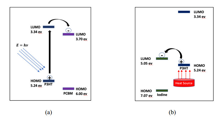
A dual doped regio-regular poly(3-hexylthiophene-2, 5-diyl) (P3HT) was investigated to develop a multi-functional organic field effect transistor (OFET). OFETs based on a pristine P3HT and a dual doped P3HT (P3HT:PCBM:I2 blend) were fabricated to study the impact of doping on the electrical properties of the samples, and to examine the mechanism through which it amplified the output performance of the doped OFETs. A series of experimental techniques such as device electrical characterization, active layer surface analysis, and photon absorptivity measurements were conducted to quantitatively characterize the principal parameters that are susceptible to change as a result of doping. Topographic mapping revealed the expected doping-induced improvements in surface morphology, which could be associated with the ability of iodine to improve interdigitation between adjacent P3HT chains. Similarly, absorption spectra showed a 3 nm red-shift of the light absorbance spectrum of the doped samples compared to the undoped samples. The electrical conductivity of the samples was also examined at various conditions of temperature and light intensity, and the values obtained from the doped sample were approximately one order of magnitude higher compared to those of the undoped sample at room temperature, which explains the reason behind the higher output current drawn from the doped device compared to that of the undoped OFET. The explanation for this is two-fold, both PCBM and iodine promote the generation of free charge carriers, which increases the electrical conductivity of the active layer; and in addition to that, the improved P3HT main-chain interdigitation brought about by the introduction of iodine results in an increase in charge-carrier mobility, which also results in higher electrical conductivity. The findings of this study offers valuable information that could be instrumental in further advancing the future organic semiconductors based studies.
Citation: Thomas Debesay, Sam-Shajing Sun, Messaoud Bahoura. Multi-functional organic field effect transistor based on a dual doped P3HT[J]. AIMS Materials Science, 2021, 8(5): 823-835. doi: 10.3934/matersci.2021050
A dual doped regio-regular poly(3-hexylthiophene-2, 5-diyl) (P3HT) was investigated to develop a multi-functional organic field effect transistor (OFET). OFETs based on a pristine P3HT and a dual doped P3HT (P3HT:PCBM:I2 blend) were fabricated to study the impact of doping on the electrical properties of the samples, and to examine the mechanism through which it amplified the output performance of the doped OFETs. A series of experimental techniques such as device electrical characterization, active layer surface analysis, and photon absorptivity measurements were conducted to quantitatively characterize the principal parameters that are susceptible to change as a result of doping. Topographic mapping revealed the expected doping-induced improvements in surface morphology, which could be associated with the ability of iodine to improve interdigitation between adjacent P3HT chains. Similarly, absorption spectra showed a 3 nm red-shift of the light absorbance spectrum of the doped samples compared to the undoped samples. The electrical conductivity of the samples was also examined at various conditions of temperature and light intensity, and the values obtained from the doped sample were approximately one order of magnitude higher compared to those of the undoped sample at room temperature, which explains the reason behind the higher output current drawn from the doped device compared to that of the undoped OFET. The explanation for this is two-fold, both PCBM and iodine promote the generation of free charge carriers, which increases the electrical conductivity of the active layer; and in addition to that, the improved P3HT main-chain interdigitation brought about by the introduction of iodine results in an increase in charge-carrier mobility, which also results in higher electrical conductivity. The findings of this study offers valuable information that could be instrumental in further advancing the future organic semiconductors based studies.

| [1] |
De Leeuw DM, Cantatore E (2008) Organic electronics: Materials, technology and circuit design developments enabling new applications. Mat Sci Semicon Proc 11: 199-204. doi: 10.1016/j.mssp.2008.10.001

|
| [2] |
Huang J, Pfeiffer M, Werner A, et al. (2002) Low-voltage organic electroluminescent devices using pin structures. Appl Phys Lett 80: 139-141. doi: 10.1063/1.1432110
|
| [3] |
Lee YH, Jang M, Lee MY, et al. (2017) Flexible field-effect transistor-type sensors based on conjugated molecules. Chem 3: 724-763. doi: 10.1016/j.chempr.2017.10.005
|
| [4] | Facchetti A (2007) Semiconductors for organic transistors. Mater Today 10: 28-37. |
| [5] |
Zhang Q, Sun Y, Xu W, et al. (2012) Thermoelectric energy from flexible P3HT films doped with a ferric salt of triflimide anions. Energ Environ Sci 5: 9639-9644. doi: 10.1039/c2ee23006b
|
| [6] |
Liu Z, Liu Q, Huang Y, et al. (2008) Organic photovoltaic devices based on a novel acceptor material: graphene. Adv Mater 20: 3924-3930. doi: 10.1002/adma.200800366
|
| [7] |
Gelinck GH, Huitema HEA, Van Veenendaal E, et al. (2004) Flexible active-matrix displays and shift registers based on solution-processed organic transistors. Nat Mater 3: 106-110. doi: 10.1038/nmat1061
|
| [8] |
Lai S, Barbaro M, Bonfiglio A (2016) Tailoring the sensing performances of an OFET-based biosensor. Sensor Actuat B-Chem 233: 314-319. doi: 10.1016/j.snb.2016.04.095
|
| [9] | Panasonic commercializes transparent OLED display module with superb image visibility. Available from: https://news.panasonic.com/global/press/data/2020/11/en201120-3/en201120-3.html. |
| [10] |
Holliday S, Ashraf RS, Wadsworth A, et al. (2016) High-efficiency and air-stable P3HT-based polymer solar cells with a new non-fullerene acceptor. Nat Commun 7: 1-11. doi: 10.1038/ncomms11585
|
| [11] |
Tiwari S, Singh AK, Joshi L, et al. (2012) Poly-3-hexylthiophene based organic field-effect transistor: Detection of low concentration of ammonia. Sensor Actuat B-Chem 171: 962-968. doi: 10.1016/j.snb.2012.06.010
|
| [12] |
Mun S, Park Y, Lee YEK, et al. (2017) Highly sensitive ammonia gas sensor based on single-crystal poly(3-hexylthiophene)(P3HT) organic field effect transistor. Langmuir 33: 13554-13560. doi: 10.1021/acs.langmuir.7b02466
|
| [13] |
Yamamoto Y, Yoshino K, Inuishi Y (1979) Electrical properties of phthalocyanine-halogen complexes. J Phys Soc Jpn 47: 1887-1891. doi: 10.1143/JPSJ.47.1887
|
| [14] |
Koopmans M, Leiviskä MA, Liu J, et al. (2020) Electrical conductivity of doped organic semiconductors limited by carrier-carrier interactions. ACS Appl Mater Inter 12: 56222-56230. doi: 10.1021/acsami.0c15490
|
| [15] |
Liang Z, Zhang Y, Souri M, et al. (2018) Influence of dopant size and electron affinity on the electrical conductivity and thermoelectric properties of a series of conjugated polymers. J Mater Chem A 6: 16495-16505. doi: 10.1039/C8TA05922E
|
| [16] |
Zhang Y, Elawad M, Yu Z, et al. (2016) Enhanced performance of perovskite solar cells with P3HT hole-transporting materials via molecular p-type doping. RSC Adv 6: 108888-108895. doi: 10.1039/C6RA21775C
|
| [17] | Lei X, Zhang F, Song T, et al. (2011) P-type doping effect on the performance of organic-inorganic hybrid solar cells. Appl Phys Lett 99: 267. |
| [18] |
Lim E, Peterson KA, Su GM, et al. (2018) Thermoelectric properties of poly (3-hexylthiophene)(P3HT) doped with 2, 3, 5, 6-Tetrafluoro-7, 7, 8, 8-tetracyanoquinodimethane (F4TCNQ) by vapor-phase infiltration. Chem Mater 30: 998-1010. doi: 10.1021/acs.chemmater.7b04849
|
| [19] | Debesay TH, Sun SS, Bahoura M (2020) A polymer composite based organic FET multi-sensing device, Organic and Hybrid Sensors and Bioelectronics XⅢ, International Society for Optics and Photonics. |
| [20] |
Debesay TH, Sun SS (2020) Phototransistors based on a lightly doped P3HT. MRS Adv 5: 1975-1982. doi: 10.1557/adv.2020.306
|
| [21] |
Aarnio H, Sehati P, Braun S, et al. (2011) Spontaneous charge transfer and dipole formation at the interface between P3HT and PCBM. Adv Energ Mater 1: 792-797. doi: 10.1002/aenm.201100074
|
| [22] |
D'Avino G, Mothy S, Muccioli L, et al. (2013) Energetics of electron-hole separation at P3HT/PCBM heterojunctions. J Phys Chem C 117: 12981-12990. doi: 10.1021/jp402957g
|
| [23] |
Clarke TM, Ballantyne AM, Nelson J, et al. (2008) Free energy control of charge photogeneration in polythiophene/fullerene solar cells: the influence of thermal annealing on P3HT/PCBM blends. Adv Funct Mater 18: 4029-4035. doi: 10.1002/adfm.200800727
|
| [24] |
Kniepert J, Lange I, Van Der Kaap NJ, et al. (2014) A conclusive view on charge generation, recombination, and extraction in as-prepared and annealed P3HT: PCBM blends: combined experimental and simulation work. Adv Energ Mater 4: 1301401. doi: 10.1002/aenm.201301401
|
| [25] |
Zhu H, Liu C, Song H, et al. (2014) Thermoelectric performance of poly(3-hexylthiophene) films doped by iodine vapor with promising high seebeck coefficient. Electron Mater Lett 10: 427-431. doi: 10.1007/s13391-013-3150-y
|
| [26] |
Tian P, Tang L, Xiang J, et al. (2016) Solution processable high-performance infrared organic photodetector by iodine doping. RSC Adv 6: 45166-45171. doi: 10.1039/C6RA02773C
|
| [27] | Zhuo Z, Zhang F, Wang J, et al. (2011) Efficiency improvement of polymer solar cells by iodine doping. Solid State Electron 63: 83-88. |
| [28] |
Lee Ⅲ HO, Sun SS (2018) Properties and mechanisms of iodine doped of P3HT and P3HT/PCBM composites. AIMS Materi Sci 5: 479-493. doi: 10.3934/matersci.2018.3.479
|


Figures(8) / Tables(1)

Thomas Debesay, Sam-Shajing Sun, Messaoud Bahoura. Multi-functional organic field effect transistor based on a dual doped P3HT[J]. AIMS Materials Science, 2021, 8(5): 823-835. doi: 10.3934/matersci.2021050


 DownLoad: