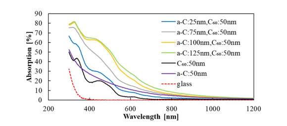
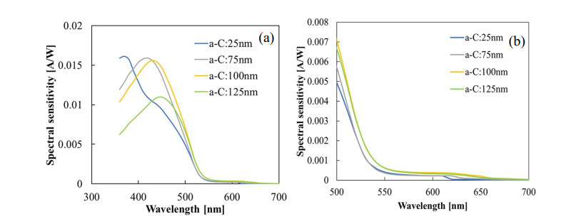
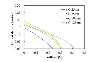
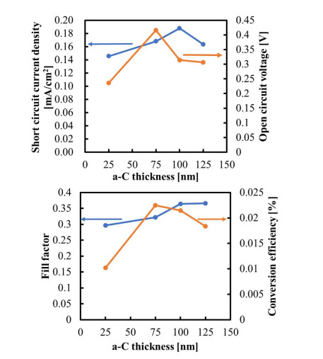
All-carbon photovoltaic devices have attracted attention in terms of resources and environment. However, the device application is very limited because of poor performance. In this work, we studied the solar cell characteristics of amorphous carbon (a–C)/fullerene (C60) junction when the thickness of the a–C layer was varied. When the thickness of the a–C layer was varied, the short-circuit current density and open-circuit voltage increased with increasing film thickness and then decreased after a certain value. Also, the spectral response measurement results suggest that most of the power generation is due to the light absorbed by the C60 layer, and that the light absorbed by the a–C layer may contribute little to power generation. This study suggests that the improvement in the electronic properties of a–C is necessary to make a photovoltaic device with high performance.
Citation: Takuto Eguchi, Shinya Kato, Naoki Kishi, Tetsuo Soga. Effect of thickness on photovoltaic properties of amorphous carbon/fullerene junction[J]. AIMS Materials Science, 2022, 9(3): 446-454. doi: 10.3934/matersci.2022026
All-carbon photovoltaic devices have attracted attention in terms of resources and environment. However, the device application is very limited because of poor performance. In this work, we studied the solar cell characteristics of amorphous carbon (a–C)/fullerene (C60) junction when the thickness of the a–C layer was varied. When the thickness of the a–C layer was varied, the short-circuit current density and open-circuit voltage increased with increasing film thickness and then decreased after a certain value. Also, the spectral response measurement results suggest that most of the power generation is due to the light absorbed by the C60 layer, and that the light absorbed by the a–C layer may contribute little to power generation. This study suggests that the improvement in the electronic properties of a–C is necessary to make a photovoltaic device with high performance.

| [1] |
Lamnatou C, Chemisana D (2017) Photovoltaic/thermal (PVT) systems: A review with emphasis on environmental issues. Renew Energ 105: 270-287. https://doi.org/10.1016/j.renene.2016.12.009 doi: 10.1016/j.renene.2016.12.009

|
| [2] | Kayes BM, Nie H, Twist R, et al. (2011) 27.6% conversion efficiency, a new record for single‐junction solar cells under 1 sun illumination, 37th IEEE Photovoltaic Specialists Conference, Seattle: IEEE, 000004-000008. https://doi.org/10.1109/PVSC.2011.6185831 |
| [3] |
Britt J, Ferekides C (1993) Thin-film CdS/CdTe solar cell with 15.8% efficiency. Appl Phys Lett 62: 2851-2852. https://doi.org/10.1063/1.109629 doi: 10.1063/1.109629
|
| [4] |
He Z, Xiao B, Liu F, et al. (2015) Single-junction polymer solar cells with high efficiency and photovoltage. Nat Photon 5: 174179. https://doi.org/10.1038/nphoton.2015.6 doi: 10.1038/nphoton.2015.6
|
| [5] |
Park NG, Grätzel M, Miyasaka T, et al. (2016) Towards stable and commercially available perovskite solar cells. Nat Energy 1: 16152. https://doi.org/10.1038/nenergy.2016.152 doi: 10.1038/nenergy.2016.152
|
| [6] |
Zhang F, Inganäs O, Zhou Y, et al. (2016) Development of polymer-fullerene solar cells. Natl Sci Rev 3: 222-239. https://doi.org/10.1093/nsr/nww020 doi: 10.1093/nsr/nww020
|
| [7] |
Tune DD, Flavel BS, Krupke R, et al. (2012) Carbon nanotube-silicon solar cells. Adv Energy Mater 2: 1043-1055. https://doi.org/10.1002/aenm.201200249 doi: 10.1002/aenm.201200249
|
| [8] |
Zhang Y, Tang TT, Girit C, et al. (2009) Direct observation of a widely tunable bandgap in bilayer graphene. Nature 459: 820-823. https://doi.org/10.1038/nature08105 doi: 10.1038/nature08105
|
| [9] |
Krishna KM, Ebisu H, Hagimoto K, et al. (2000) Low density of defect states in hydrogenated amorphous carbon thin films grown by plasma-enhanced chemical vapor deposition. Appl Phys Lett 78: 294-296. https://doi.org/10.1063/1.1335548 doi: 10.1063/1.1335548
|
| [10] |
Zkria A, Abdel-Wahab F, Katamune Y, et al. (2018) Optical and structural characterization of ultrananocrystalline diamond/hydrogenated amorphous carbon composite films deposited via coaxial arc plasma. Curr Appl Phys 19: 143-148. https://doi.org/10.1016/j.cap.2018.11.012 doi: 10.1016/j.cap.2018.11.012
|
| [11] |
Zarei Moghadam R, Rezagholipour Dizaji H, Ehsani MH (2019) Modification of optical and mechanical properties of nitrogen doped diamond-like carbon layers. J Mater Sci-mater El 30: 19770-19781. https://doi.org/10.1007/s10854-019-02343-4 doi: 10.1007/s10854-019-02343-4
|
| [12] |
Wojciechowski K, Leijtens T, Siprova S, et al. (2015) C60 as an efficient n-type compact layer in perovskite solar cells. J Phys Chem Lett 6: 2399-2405. https://doi.org/10.1021/acs.jpclett.5b00902 doi: 10.1021/acs.jpclett.5b00902
|
| [13] |
Chhowalla M, Robertson J, Chen CW (1997) Influence of ion energy and substrate temperature on the optical and electronic properties of tetrahedral amorphous carbon (ta-C) films. J Appl Phys 81: 139-145. https://doi.org/10.1063/1.364000 doi: 10.1063/1.364000
|
| [14] |
Alves MAR, Rossetto JF, Balachova O, et al. (2001) Some optical properties of amorphous hydrogenated carbon thin films prepared by rf plasma deposition using methane. Microelectronics J 32: 783-786. https://doi.org/10.1016/S0026-2692(01)00046-5 doi: 10.1016/S0026-2692(01)00046-5
|
| [15] |
Yu FA, Kaneko T, Yoshimura S, et al. (1996) The spectro‐photovoltaic characteristics of a carbonaceous film/n‐type silicon (C/n-Si) photovoltaic cell. Appl Phys Lett 69: 4078-4080. https://doi.org/10.1063/1.117825 doi: 10.1063/1.117825
|
| [16] |
Ma M, Xue Q, Chen H, et al. (2010) Photovoltaic characteristics of Pd doped amorphous carbon film/SiO2/Si. Appl Phys Lett 97: 061902. https://doi.org/10.1063/1.3478230 doi: 10.1063/1.3478230
|
| [17] |
Soga T, Kokubu T, Hayashi Y, et al. (2005) Effect of rf power on the photovoltaic properties of boron-doped amorphous carbon/n-type silicon junction fabricated by plasma enhanced chemical vapor deposition. Thin Solid Films 482: 86-89. https://doi.org/10.1016/j.tsf.2004.11.123 doi: 10.1016/j.tsf.2004.11.123
|
| [18] |
Ma ZQ, Liu BX (2001) Boron-doped diamond-like amorphous carbon as photovoltaic films in solar cell. Sol Energy Mater Sol Cells 69: 339-344. https://doi.org/10.1016/S0927-0248(00)00400-1 doi: 10.1016/S0927-0248(00)00400-1
|
| [19] |
Zhu H, Wei J, Wang K, et al. (2009) Applications of carbon materials in photovoltaic solar cells. Sol Energy Mater Sol Cells 93: 1461-1470. https://doi.org/10.1016/j.solmat.2009.04.006 doi: 10.1016/j.solmat.2009.04.006
|
| [20] |
Chen J, Song QL, Xiong ZH, et al. (2011) Environment-friendly energy from all-carbon solar cells based on fullerene-C60. Sol Energy Mater Sol Cells 95: 1138-1140. https://doi.org/10.1016/j.solmat.2010.12.037 doi: 10.1016/j.solmat.2010.12.037
|
| [21] |
Kubo M, Kaji T, Hiramoto M (2011) pn-homojunction formation in single fullerene films. AIP Adv 1: 032177. https://doi.org/10.1063/1.3647994 doi: 10.1063/1.3647994
|
| [22] |
Tung VC, Huang JH, Kim J, et al. (2012) Towards solution processed all-carbon solar cells: a perspective. Energy Environ Sci 5: 7810-7818. https://doi.org/10.1039/C2EE21587J doi: 10.1039/C2EE21587J
|
| [23] |
Nagata A, Oku T, Suzuki A, et al. (2010) Fabrication and photovoltaic property of diamond: fullerene nanocomposite thin films. J Ceram Soc Jpn 118: 1006-1008. https://doi.org/10.2109/jcersj2.118.1006 doi: 10.2109/jcersj2.118.1006
|
| [24] |
Soga T, Kondoh T, Kishi N, et al. (2013) Photovoltaic properties of an amorphous carbon/fullerene junction. Carbon 60: 1-4. https://doi.org/10.1016/j.carbon.2013.02.050 doi: 10.1016/j.carbon.2013.02.050
|
| [25] |
Kato H, Yamamoto Y, Kato S, et al. (2018) Fabrication and evaluation of two-junction carbon thin film photovoltaic devices. J Solar Eneg Res Updat 5: 1-7. http://dx.doi.org/10.15377/2410-2199.2018.05.1 doi: 10.15377/2410-2199.2018.05.1
|
| [26] |
Soga T, Kishi N (2019) Improved photovoltaic properties of amorphous carbon/fullerene junction by nitrogen doping. J Mater Sci-mater El 30: 6628-6632. https://doi.org/10.1007/s10854-019-00970-5 doi: 10.1007/s10854-019-00970-5
|
| [27] |
Bogdanov AA (2018) Absorption spectra of C60 fullerene monomolecular films. Tech Phy 63: 1006-1009. https://doi.org/10.1134/S1063784218070083 doi: 10.1134/S1063784218070083
|
| [28] |
Katsuno T, Nitta S, Habuchi H, et al. (2004) Highly photoconductive amorphous carbon nitride films prepared by cyclic nitrogen radical sputtering. Appl Phys Lett 85: 2803-2805. https://doi.org/10.1063/1.1792384 doi: 10.1063/1.1792384
|
| [29] |
Yang X, Zhao L, Wang S, et al. (2021) Recent progress of g-C3N4 applied in solar cells. J Materiomics 7: 728-741. https://doi.org/10.1016/j.jmat.2021.01.004 doi: 10.1016/j.jmat.2021.01.004
|
Figures(6) / Tables(1)

Takuto Eguchi, Shinya Kato, Naoki Kishi, Tetsuo Soga. Effect of thickness on photovoltaic properties of amorphous carbon/fullerene junction[J]. AIMS Materials Science, 2022, 9(3): 446-454. doi: 10.3934/matersci.2022026


 DownLoad: