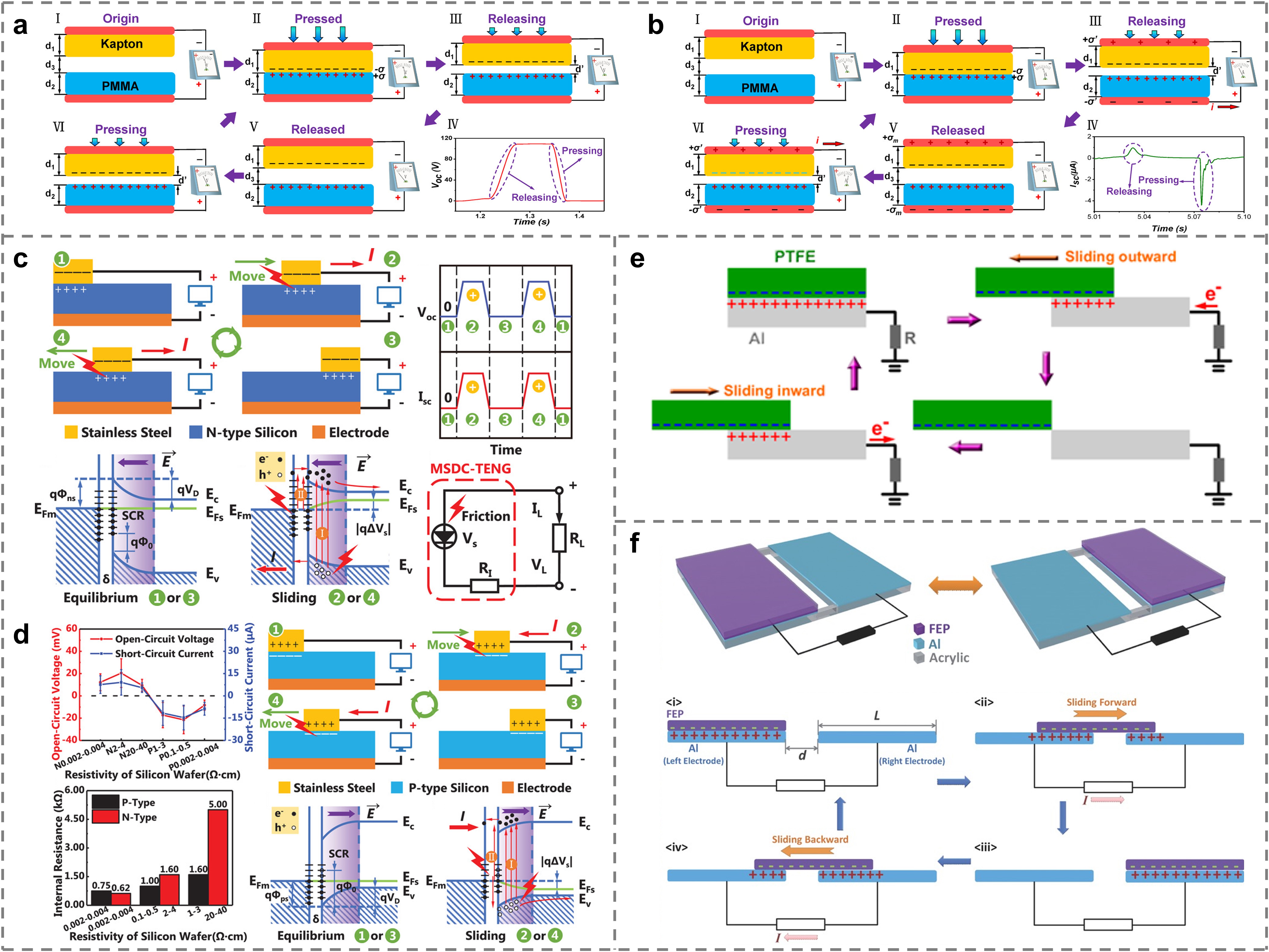
The triboelectric nanogenerator (TENG), as a new energy harvesting device, can efficiently harvest mechanical energy from the environment to provide continuous power for electronic devices, which has great potential for powering intelligent distributed network. Laser processing technology, which enables structural, phase, and property control at different scales, can quickly and easily complete the surface patterning of TENG and facilitate efficient energy harvesting. In this work, we outline the working modes and principles of TENG, review the research progress of laser surface processing technology for fabricating TENG in recent years, including laser-induced graphene (LIG), laser ablation, laser carbonization, laser-induced copper, etc., and perspectives on the challenges and future directions for development of laser surface processing for performance enhancement of TENG.
Citation: Jia Tian, Yue He, Fangpei Li, Wenbo Peng, Yongning He. Laser surface processing technology for performance enhancement of TENG[J]. AIMS Materials Science, 2025, 12(1): 1-22. doi: 10.3934/matersci.2025001
The triboelectric nanogenerator (TENG), as a new energy harvesting device, can efficiently harvest mechanical energy from the environment to provide continuous power for electronic devices, which has great potential for powering intelligent distributed network. Laser processing technology, which enables structural, phase, and property control at different scales, can quickly and easily complete the surface patterning of TENG and facilitate efficient energy harvesting. In this work, we outline the working modes and principles of TENG, review the research progress of laser surface processing technology for fabricating TENG in recent years, including laser-induced graphene (LIG), laser ablation, laser carbonization, laser-induced copper, etc., and perspectives on the challenges and future directions for development of laser surface processing for performance enhancement of TENG.

| [1] |
Wang ZL (2019) Entropy theory of distributed energy for internet of things. Nano Energy 58: 669–672. https://doi.org/10.1016/j.nanoen.2019.02.012 doi: 10.1016/j.nanoen.2019.02.012

|
| [2] |
Fan FR, Tian ZQ, Wang ZL (2012) Flexible triboelectric generator. Nano Energy 1: 328–334. https://doi.org/10.1016/j.nanoen.2012.01.004 doi: 10.1016/j.nanoen.2012.01.004
|
| [3] |
Li Y, Yu J, Wei Y, et al. (2023) Recent progress in self-powered wireless sensors and systems based on TENG. Sensors 23: 1329. https://doi.org/10.3390/s23031329 doi: 10.3390/s23031329
|
| [4] |
Wu Z, Cheng T, Wang ZL (2020) Self-powered sensors and systems based on nanogenerators. Sensors 20: 2925. https://doi.org/10.3390/s20102925 doi: 10.3390/s20102925
|
| [5] |
Shen J, Li B, Yang Y, et al. (2022) Application, challenge and perspective of triboelectric nanogenerator as micro-nano energy and self-powered biosystem. Biosens Bioelectron 216: 114595. https://doi.org/10.1016/j.bios.2022.114595 doi: 10.1016/j.bios.2022.114595
|
| [6] |
Shi Q, He T, Lee C (2019) More than energy harvesting-combining triboelectric nanogenerator and flexible electronics technology for enabling novel micro-/nano-systems. Nano Energy 57: 851–871. https://doi.org/10.1016/j.nanoen.2019.01.002 doi: 10.1016/j.nanoen.2019.01.002
|
| [7] |
Sun J, Zhang L, Gong S, et al. (2024) Device physics and application prospect of the emerging high-voltage supply technology arising from triboelectric nanogenerator. Nano Energy 119: 109010. https://doi.org/10.1016/j.nanoen.2023.109010 doi: 10.1016/j.nanoen.2023.109010
|
| [8] |
Wang X, Chen X, Iwamoto M (2020) Recent progress in the development of portable high voltage source based on triboelectric nanogenerator. Smart Mater Med 1: 66–76. https://doi.org/10.1016/j.smaim.2020.07.002 doi: 10.1016/j.smaim.2020.07.002
|
| [9] |
Wang ZL, Jiang T, Xu L (2017) Toward the blue energy dream by triboelectric nanogenerator networks. Nano Energy 39: 9–23. https://doi.org/10.1016/j.nanoen.2017.06.035 doi: 10.1016/j.nanoen.2017.06.035
|
| [10] |
Chen J, Yang J, Li Z, et al. (2015) Networks of triboelectric nanogenerators for harvesting water wave energy: A potential approach toward blue energy. ACS Nano 9: 3324–3331. https://doi.org/10.1021/acsnano.5b00534 doi: 10.1021/acsnano.5b00534
|
| [11] |
Li XF, Berbille A, Wang TY, et al. (2024) Defect passivation toward designing high-performance fluorinated polymers for liquid-solid contact-electrification and contact-electro-catalysis. Adv Funct Mater 34: 2315817. https://doi.org/10.1002/adfm.202315817 doi: 10.1002/adfm.202315817
|
| [12] |
Han K, Luo J, Feng Y, et al. (2020) Self-powered electrocatalytic ammonia synthesis directly from air as driven by dual triboelectric nanogenerators. Energy Environ Sci 13: 2450–2458. https://doi.org/10.1039/D0EE01102A doi: 10.1039/D0EE01102A
|
| [13] |
Corrielli G, Crespi A, Osellame R (2021) Femtosecond laser micromachining for integrated quantum photonics. Nanophotonics 10: 3789–3812. https://doi.org/10.1515/nanoph-2021-0419 doi: 10.1515/nanoph-2021-0419
|
| [14] |
Lin Z, Hong M (2021) Femtosecond laser precision engineering: From micron, submicron, to nanoscale. Ultrafast Sci 2021: 783514. https://doi.org/10.34133/2021/9783514 doi: 10.34133/2021/9783514
|
| [15] |
Jia Y, Chen F (2023) Recent progress on femtosecond laser micro-/nano-fabrication of functional photonic structures in dielectric crystals: A brief review and perspective. APL Photonics 8: 090901. https://doi.org/10.1063/5.0160067 doi: 10.1063/5.0160067
|
| [16] |
Phan H, Hoa PN, Tam HA, et al. (2021) Q-switched pulsed laser direct writing of aluminum surface micro/nanostructure for triboelectric performance enhancement. J Sci-Adv Mater Dev 6: 84–91. https://doi.org/10.1016/j.jsamd.2020.11.003 doi: 10.1016/j.jsamd.2020.11.003
|
| [17] |
dos Santos A, Sabino F, Rovisco A, et al. (2021) Optimization of ZnO nanorods concentration in a micro-structured polymeric composite for nanogenerators. Chemosensors 9: 27. https://doi.org/10.3390/chemosensors9020027 doi: 10.3390/chemosensors9020027
|
| [18] |
Muthu M, Pandey R, Wang X, et al. (2020) Enhancement of triboelectric nanogenerator output performance by laser 3D-Surface pattern method for energy harvesting application. Nano Energy 78: 105205. https://doi.org/10.1016/j.nanoen.2020.105205 doi: 10.1016/j.nanoen.2020.105205
|
| [19] |
Wang R, Gao S, Yang Z, et al. (2018) Engineered and laser‐processed chitosan biopolymers for sustainable and biodegradable triboelectric power generation. Adv Mater 30: 1706267. https://doi.org/10.1002/adma.201706267 doi: 10.1002/adma.201706267
|
| [20] |
Guo W, Xia Y, Zhu Y, et al. (2023) Laser-induced graphene based triboelectric nanogenerator for accurate wireless control and tactile pattern recognition. Nano Energy 108: 108229. https://doi.org/10.1016/j.nanoen.2023.108229 doi: 10.1016/j.nanoen.2023.108229
|
| [21] |
Zhu G, Pan C, Guo W, et al. (2012) Triboelectric-generator-driven pulse electrodeposition for micropatterning. Nano Lett 12: 4960–4965. https://doi.org/10.1021/nl302560k doi: 10.1021/nl302560k
|
| [22] |
Zhang Z, Jiang D, Zhao J, et al. (2020) Tribovoltaic effect on metal-semiconductor interface for direct-current low-impedance triboelectric nanogenerators. Adv Energy Mater 10: 1903713. https://doi.org/10.1002/aenm.201903713 doi: 10.1002/aenm.201903713
|
| [23] |
Yang Y, Zhang H, Chen J, et al. (2013) Single-electrode-based sliding triboelectric nanogenerator for self-powered displacement vector sensor system. ACS Nano 7: 7342–7351. https://doi.org/10.1021/nn403021m doi: 10.1021/nn403021m
|
| [24] |
Wang S, Xie Y, Niu S, et al. (2014) Freestanding triboelectric-layer-based nanogenerators for harvesting energy from a moving object or human motion in contact and non-contact modes. Adv Mater 26: 2818–2824. https://doi.org/10.1002/adma.201305303 doi: 10.1002/adma.201305303
|
| [25] |
Zhang H, Yang Y, Su Y, et al. (2013) Triboelectric nanogenerator for harvesting vibration energy in full space and as self‐powered acceleration sensor. Adv Funct Mater 24: 1401–1407. https://doi.org/10.1002/adfm.201302453 doi: 10.1002/adfm.201302453
|
| [26] |
Bae J, Lee J, Kim S, et al. (2014) Flutter-driven triboelectrification for harvesting wind energy. Nat Commun 5: 4929. https://doi.org/10.1038/ncomms5929 doi: 10.1038/ncomms5929
|
| [27] |
Wang J, Wu C, Dai Y, et al. (2017) Achieving ultrahigh triboelectric charge density for efficient energy harvesting. Nat Commun 8: 88. https://doi.org/10.1038/s41467-017-00131-4 doi: 10.1038/s41467-017-00131-4
|
| [28] |
Qin H, Xu L, Lin S, et al. (2022) Underwater energy harvesting and sensing by sweeping out the charges in an electric double layer using an oil droplet. Adv Funct Mater 32: 2111662. https://doi.org/10.1002/adfm.202111662 doi: 10.1002/adfm.202111662
|
| [29] |
Zhang B, Gao Q, Li W, et al. (2023) Alternating magnetic field-enhanced triboelectric nanogenerator for low-speed flow energy harvesting. Adv Funct Mater 33: 2304839. https://doi.org/10.1002/adfm.202304839 doi: 10.1002/adfm.202304839
|
| [30] |
Chen BD, Tang W, He C, et al. (2017) Ultrafine capillary-tube triboelectric nanogenerator as active sensor for microliquid biological and chemical sensing. Adv Mater Technol 3: 1700229. https://doi.org/10.1002/admt.201700229 doi: 10.1002/admt.201700229
|
| [31] |
Ying S, Zhang J, Yan K, et al. (2021) Self-powered direct-current type pressure sensor by polypyrrole/metal Schottky junction. J Phys D Appl Phys 54: 424008. https://doi.org/10.1088/1361-6463/ac196c doi: 10.1088/1361-6463/ac196c
|
| [32] |
Liu J, Wen Z, Lei H, et al. (2022) A liquid-solid interface-based triboelectric tactile sensor with ultrahigh sensitivity of 21.48 kPa-1. Nano-Micro Lett 14: 88. https://doi.org/10.1007/s40820-022-00831-7 doi: 10.1007/s40820-022-00831-7
|
| [33] |
Yang Y, Zhang H, Lin ZH, et al. (2013) Human skin based triboelectric nanogenerators for harvesting biomechanical energy and as self-powered active tactile sensor system. ACS Nano 7: 9213–9222. https://doi.org/10.1021/nn403838y doi: 10.1021/nn403838y
|
| [34] |
Bagchi B, Datta P, Fernandez CS, et al. (2023) Flexible triboelectric nanogenerators using transparent copper nanowires electrodes: Energy harvesting, sensing human activities and material recognition. Mater Horiz 10: 3124–3134. https://doi.org/10.1039/D3MH00404J doi: 10.1039/D3MH00404J
|
| [35] |
Song T, Jiang S, Cai N, et al. (2023) A strategy for human safety monitoring in high-temperature environments by 3D-printed heat-resistant TENG sensors. Chem Eng J 475: 146292. https://doi.org/10.1016/j.cej.2023.146292 doi: 10.1016/j.cej.2023.146292
|
| [36] |
Qi C, Yang Z, Zhi J, et al. (2023) Enhancing the powering ability of triboelectric nanogenerator through output signal's management strategies. Nano Res 16: 11783–11800. https://doi.org/10.1007/s12274-023-5834-4 doi: 10.1007/s12274-023-5834-4
|
| [37] |
Zou H, Zhang Y, Guo L, et al. (2019) Quantifying the triboelectric series. Nat Commun 10: 1427. https://doi.org/10.1038/s41467-019-09461-x doi: 10.1038/s41467-019-09461-x
|
| [38] |
Zhang J, Rogers FJM, Darwish N, et al. (2019) Electrochemistry on tribocharged polymers is governed by the stability of surface charges rather than charging magnitude. J Am Chem Soc 141: 5863–5870. https://doi.org/10.1021/jacs.9b00297 doi: 10.1021/jacs.9b00297
|
| [39] |
Baytekin HT, Patashinski AZ, Branicki M, et al. (2011) The mosaic of surface charge in contact electrification. Science 333: 308–312. https://doi.org/10.1126/science.1201512 doi: 10.1126/science.1201512
|
| [40] |
Sobolev YI, Adamkiewicz W, Siek M, et al. (2022) Charge mosaics on contact-electrified dielectrics result from polarity-inverting discharges. Nat Phys 18: 1347–1355. https://doi.org/10.1038/s41567-022-01714-9 doi: 10.1038/s41567-022-01714-9
|
| [41] |
Wang J, Xu S, Hu C (2024) Charge generation and enhancement of key components of triboelectric nanogenerators: A review. Adv Mater 36: 2409833. https://doi.org/10.1002/adma.202409833 doi: 10.1002/adma.202409833
|
| [42] |
Wu H, He W, Shan C, et al. (2022) Achieving remarkable charge density via self-polarization of polar high-k material in a charge-excitation triboelectric nanogenerator. Adv Mater 34: 2109918. https://doi.org/10.1002/adma.202109918 doi: 10.1002/adma.202109918
|
| [43] |
Shin SH, Bae YE, Moon HK, et al. (2017) Formation of triboelectric series via atomic-level surface functionalization for triboelectric energy harvesting. ACS Nano 11: 6131–6138. https://doi.org/10.1021/acsnano.7b02156 doi: 10.1021/acsnano.7b02156
|
| [44] |
Biegaj KW, Rowland MG, Lukas TM, et al. (2017) Surface chemistry and humidity in powder electrostatics: a comparative study between tribocharging and corona discharge. ACS Omega 2: 1576–1582. https://doi.org/10.1021/acsomega.7b00125 doi: 10.1021/acsomega.7b00125
|
| [45] |
Wang S, Xie Y, Niu S, et al. (2014) Maximum surface charge density for triboelectric nanogenerators achieved by ionized-air injection: Methodology and theoretical understanding. Adv Mater 26: 6720–6728. https://doi.org/10.1002/adma.201402491 doi: 10.1002/adma.201402491
|
| [46] |
Li S, Fan Y, Chen H, et al. (2020) Manipulating the triboelectric surface charge density of polymers by low-energy helium ion irradiation/implantation. Energy Environ Sci 13: 896–907. https://doi.org/10.1039/C9EE03307F doi: 10.1039/C9EE03307F
|
| [47] |
Chen SN, Chen CH, Lin ZH, et al. (2018) On enhancing capability of tribocharge transfer of ZnO nanorod arrays by Sb doping for anomalous output performance improvement of triboelectric nanogenerators. Nano Energy 45: 311–318. https://doi.org/10.1016/j.nanoen.2018.01.013 doi: 10.1016/j.nanoen.2018.01.013
|
| [48] | Guo QZ, Yang LC, Wang RC, et al. Tunable work function of MgxZn1-xO as a viable friction material for a triboelectric nanogenerator. ACS Appl Mater Interfaces 11: 1420–1425. https://doi.org/10.1021/acsami.8b17416 |
| [49] |
Feng H, Li H, Xu J, et al. (2022) Triboelectric nanogenerator based on direct image lithography and surface fluorination for biomechanical energy harvesting and self-powered sterilization. Nano Energy 98: 107279. https://doi.org/10.1016/j.nanoen.2022.107279 doi: 10.1016/j.nanoen.2022.107279
|
| [50] |
Hong D, Choi YM, Jang Y, et al. (2018) A multilayer thin-film screen-printed triboelectric nanogenerator. Int J Energy Res 42: 3688–3695. https://doi.org/10.1002/er.4092 doi: 10.1002/er.4092
|
| [51] |
Zhang C, Zhang L, Bao B, et al. (2022) Customizing triboelectric nanogenerator on everyday clothes by screen-printing technology for biomechanical energy harvesting and human-interactive applications. Adv Mater Technol 8: 2201138. https://doi.org/10.1002/admt.202201138 doi: 10.1002/admt.202201138
|
| [52] |
Luo J, Fan FR, Jiang T, et al. (2015) Integration of micro-supercapacitors with triboelectric nanogenerators for a flexible self-charging power unit. Nano Res 8: 3934–3943. https://doi.org/10.1007/s12274-015-0894-8 doi: 10.1007/s12274-015-0894-8
|
| [53] |
Jin S, Wang Y, Motlag M, et al. (2018) Large-area direct laser-shock imprinting of a 3D biomimic hierarchical metal surface for triboelectric nanogenerators. Adv Mater 30: 1705840. https://doi.org/10.1002/adma.201705840 doi: 10.1002/adma.201705840
|
| [54] |
Qi D, Liu Y, Liu Z, et al. (2016) Design of architectures and materials in in-plane micro-supercapacitors: current status and future challenges. Adv Mater 29: 1602802. https://doi.org/10.1002/adma.201602802 doi: 10.1002/adma.201602802
|
| [55] |
Liu H, Sun Z, Chen Y, et al. (2022) Laser processing of flexible in-plane micro-supercapacitors: progresses in advanced manufacturing of nanostructured electrodes. ACS Nano 16: 10088–10129. https://doi.org/10.1021/acsnano.2c02812 doi: 10.1021/acsnano.2c02812
|
| [56] |
Liu X, Du D, Mourou G (2002) Laser ablation and micromachining with ultrashort laser pulses. Ieee J Quantum Elect 33: 1706–1716. https://doi.org/10.1109/3.631270 doi: 10.1109/3.631270
|
| [57] |
Wang S, Yang J, Deng G, et al. (2024) Femtosecond laser direct writing of flexible electronic devices: A mini review. Materials 17: 557. https://doi.org/10.3390/ma17030557 doi: 10.3390/ma17030557
|
| [58] |
Yang D, Zhang L, Luo N, et al. (2022) Tribological-behaviour-controlled direct-current triboelectric nanogenerator based on the tribovoltaic effect under high contact pressure. Nano Energy 99: 107370. https://doi.org/10.1016/j.nanoen.2022.107370 doi: 10.1016/j.nanoen.2022.107370
|
| [59] |
Lee YS, Jeon S, Kim D, et al. (2023) High performance direct current-generating triboelectric nanogenerators based on tribovoltaic p-n junction with ChCl-passivated CsFAMA perovskite. Nano Energy 106: 108066. https://doi.org/10.1016/j.nanoen.2022.108066 doi: 10.1016/j.nanoen.2022.108066
|
| [60] |
Lin J, Peng Z, Liu Y, et al. (2014) Laser-induced porous graphene films from commercial polymers. Nat Commun 5: 5714. https://doi.org/10.1038/ncomms6714 doi: 10.1038/ncomms6714
|
| [61] |
Xia SY, Long Y, Huang Z, et al. (2022) Laser-induced graphene (LIG)-based pressure sensor and triboelectric nanogenerator towards high-performance self-powered measurement-control combined system. Nano Energy 96: 107099. https://doi.org/10.1109/FLEPS53764.2022.9781522 doi: 10.1109/FLEPS53764.2022.9781522
|
| [62] |
Choi KH, Park S, Hyeong SK, et al. (2020) Triboelectric effect of surface morphology controlled laser induced graphene. J Mater Chem A 8: 19822–19832. https://doi.org/10.1039/D0TA05806H doi: 10.1039/D0TA05806H
|
| [63] |
Zhao P, Bhattacharya G, Fishlock SJ, et al. (2020) Replacing the metal electrodes in triboelectric nanogenerators: High-performance laser-induced graphene electrodes. Nano Energy 75: 104958. https://doi.org/10.1016/j.nanoen.2020.104958 doi: 10.1016/j.nanoen.2020.104958
|
| [64] |
Yan Z, Wang L, Xia Y, et al. (2021) Flexible high-resolution triboelectric sensor array based on patterned laser-induced graphene for self-powered real-time tactile sensing. Adv Funct Mater 31: 2100709. https://doi.org/10.1002/adfm.202100709 doi: 10.1002/adfm.202100709
|
| [65] |
Yan J, Wang H, Wang X, et al. (2024) High-performance triboelectric nanogenerators with laser-induced graphene pattern for efficient charge transfer. Appl Surf Sci 661: 160034. https://doi.org/10.1016/j.apsusc.2024.160034 doi: 10.1016/j.apsusc.2024.160034
|
| [66] |
Li JT, Stanford MG, Chen W, et al. (2020) Laminated laser-induced graphene composites. ACS Nano 14: 7911–7919. https://doi.org/10.1021/acsnano.0c02835 doi: 10.1021/acsnano.0c02835
|
| [67] | Phipps CR (2007) Laser ablation and its applications, In: Phipps C, Contributions to Laser ablation, 1 Eds., New York: Springer, 281–298. |
| [68] |
Li Y, Zhou X, Qi W, et al. (2020) Ultrafast fabrication of Cu oxide micro/nano-structures via laser ablation to promote oxygen evolution reaction. Chem Eng J 383: 123086. https://doi.org/10.1016/j.cej.2019.123086 doi: 10.1016/j.cej.2019.123086
|
| [69] |
Shiby S, Kaushik S, Gupta P, et al. (2023) Influence of laser wavelength in simultaneous patterning of fluorinated ethylene propylene and copper electrode surface towards performance enhancement of triboelectric nanogenerator. Energy Technol 11: 2300482. https://doi.org/10.1002/ente.202300482 doi: 10.1002/ente.202300482
|
| [70] |
Lee K, Mhin S, Han H, et al. (2022) A high-performance PDMS-based triboelectric nanogenerator fabricated using surface-modified carbon nanotubes via pulsed laser ablation. J Mater Chem A 10: 1299–1308. https://doi.org/10.1039/D1TA08414C doi: 10.1039/D1TA08414C
|
| [71] |
Lee K, Han H, Ryu JH, et al. (2023) Laser-driven formation of ZnSnO3/CNT heterostructure and its critical role in boosting performance of the triboelectric nanogenerator. Carbon 212: 118120. https://doi.org/10.1016/j.carbon.2023.118120 doi: 10.1016/j.carbon.2023.118120
|
| [72] |
Trinh VL, Chung CK (2017) A facile method and novel mechanism using microneedle-structured PDMS for triboelectric generator applications. Small 13: 1700373. https://doi.org/10.1002/smll.201700373 doi: 10.1002/smll.201700373
|
| [73] |
Kim D, Tcho IW, Jin IK, et al. (2017) Direct-laser-patterned friction layer for the output enhancement of a triboelectric nanogenerator. Nano Energy 35: 379–386. https://doi.org/10.1016/j.nanoen.2017.04.013 doi: 10.1016/j.nanoen.2017.04.013
|
| [74] |
Cho H, Jo S, Kim I, et al. (2021) Film-sponge-coupled triboelectric nanogenerator with enhanced contact area based on direct ultraviolet laser ablation. ACS Appl Mater Interfaces 13: 48281–48291. https://doi.org/10.1021/acsami.1c14572 doi: 10.1021/acsami.1c14572
|
| [75] |
Huang J, Fu X, Liu G, et al. (2019) Micro/nano-structures-enhanced triboelectric nanogenerators by femtosecond laser direct writing. Nano Energy 62: 638–644. https://doi.org/10.1016/j.nanoen.2019.05.081 doi: 10.1016/j.nanoen.2019.05.081
|
| [76] |
Salauddin M, Rana SMS, Sharifuzzaman M, et al. (2022) Laser-carbonized MXene/ZiF-67 nanocomposite as an intermediate layer for boosting the output performance of fabric-based triboelectric nanogenerator. Nano Energy 100: 107462. https://doi.org/10.1016/j.nanoen.2022.107462 doi: 10.1016/j.nanoen.2022.107462
|
| [77] |
Zhu S, Xia Y, Zhu Y, et al. (2022) High-performance triboelectric nanogenerator powered flexible electroluminescence devices based on patterned laser-induced copper electrodes for visualized information interaction. Nano Energy 96: 107116. https://doi.org/10.1016/j.nanoen.2022.107116 doi: 10.1016/j.nanoen.2022.107116
|
| [78] |
Qi Y, Kuang Y, Liu Y, et al. (2022) Kirigami-inspired triboelectric nanogenerator as ultra-wide-band vibrational energy harvester and self-powered acceleration sensor. Appl Energy 327: 120092. https://doi.org/10.1016/j.apenergy.2022.120092 doi: 10.1016/j.apenergy.2022.120092
|
| [79] |
Mishra S, Rakshita M, Divi H, et al. (2023) Unique contact point modification technique for boosting the performance of a triboelectric nanogenerator and its application in road safety sensing and detection. ACS Appl Mater Interfaces 15: 33095–33108. https://doi.org/10.1021/acsami.3c04848 doi: 10.1021/acsami.3c04848
|
| [80] |
Park S, Park J, Kim YG, et al. (2020) Laser-directed synthesis of strain-induced crumpled MoS2 structure for enhanced triboelectrification toward haptic sensors. Nano Energy 78: 105266. https://doi.org/10.1016/j.nanoen.2020.105266 doi: 10.1016/j.nanoen.2020.105266
|
| [81] |
Nian Q, Saei M, Xu Y, et al. (2015) Crystalline nanojoining silver nanowire percolated networks on flexible substrate. ACS Nano 9: 10018–10031. https://doi.org/10.1021/acsnano.5b03601 doi: 10.1021/acsnano.5b03601
|
| [82] | Ryoo G, Lee B, Shin S, et al. (2023) Laser-assisted interfacial engineering for high-performance all-solid-state batteries. ChemElectroChem 10: e202300349. https://doi.org/10.1002/celc.202300349 |
| [83] |
Van Hooreweder B, Moens D, Boonen R, et al. (2013) On the difference in material structure and fatigue properties of nylon specimens produced by injection molding and selective laser sintering. Polym Test 32: 972–981. https://doi.org/10.1016/j.polymertesting.2013.04.014 doi: 10.1016/j.polymertesting.2013.04.014
|
| [84] |
Trusovas R, Račiukaitis G, Niaura G, et al. (2015) Recent advances in laser utilization in the chemical modification of graphene oxide and its applications. Adv Opt Mater 4: 37–65. https://doi.org/10.1002/adom.201500469 doi: 10.1002/adom.201500469
|


Figures(5) / Tables(4)

Jia Tian, Yue He, Fangpei Li, Wenbo Peng, Yongning He. Laser surface processing technology for performance enhancement of TENG[J]. AIMS Materials Science, 2025, 12(1): 1-22. doi: 10.3934/matersci.2025001


 DownLoad: