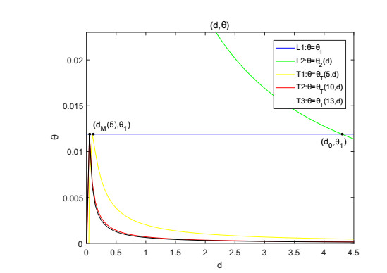
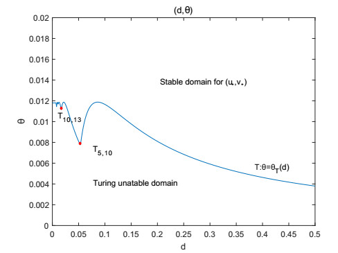
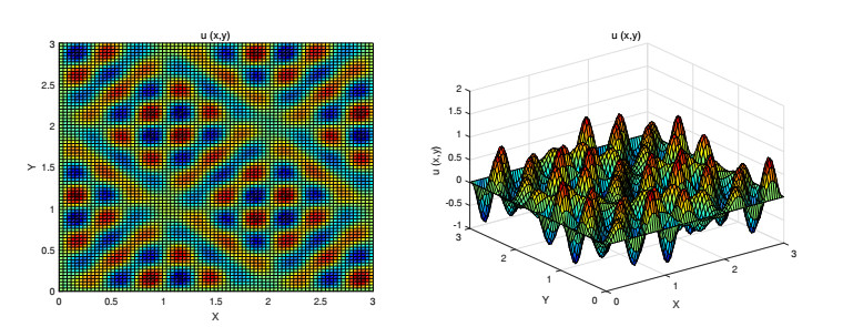
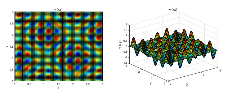
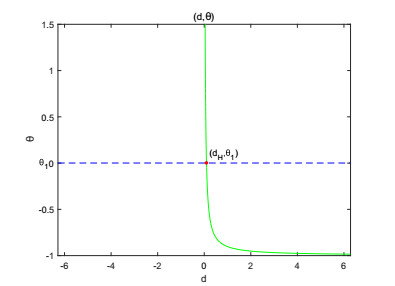
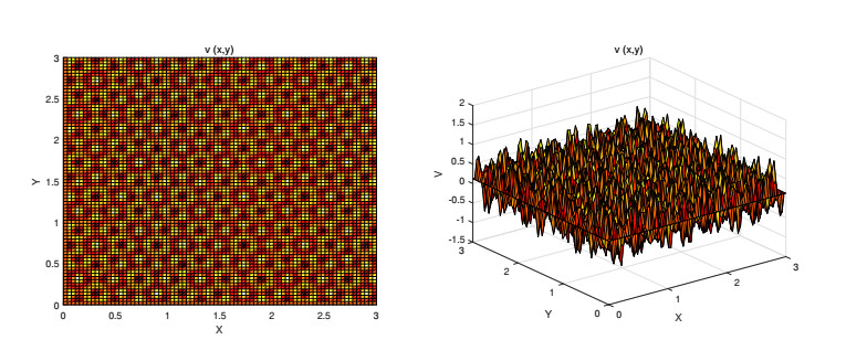
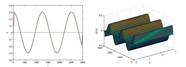
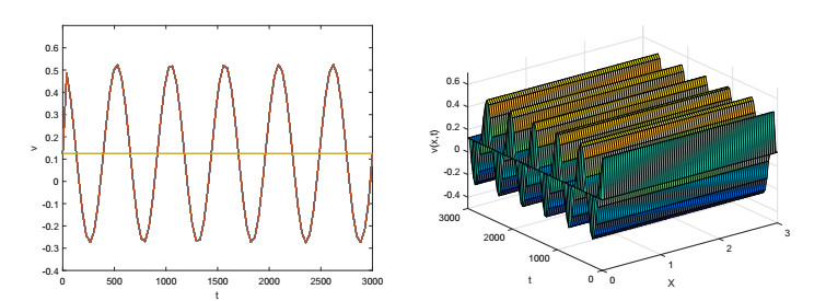
On the basis of logistic models of forest restoration, we consider the influence of population pressure on forest restoration and establish a reaction diffusion model with Holling Ⅱ functional responses. We study this reaction diffusion model under Dirichlet boundary conditions and obtain a positive equilibrium. In the square region, we analyze the existence of Turing instability and Hopf bifurcation near this point. The square patterns and mixed patterns are obtained when steady-state bifurcation occurs, the hyperhexagonal patterns appears in Hopf bifurcation.
Citation: Mingzhu Qu, Chunrui Zhang, Xingjian Wang. Analysis of dynamic properties on forest restoration-population pressure model[J]. Mathematical Biosciences and Engineering, 2020, 17(4): 3567-3581. doi: 10.3934/mbe.2020201
On the basis of logistic models of forest restoration, we consider the influence of population pressure on forest restoration and establish a reaction diffusion model with Holling Ⅱ functional responses. We study this reaction diffusion model under Dirichlet boundary conditions and obtain a positive equilibrium. In the square region, we analyze the existence of Turing instability and Hopf bifurcation near this point. The square patterns and mixed patterns are obtained when steady-state bifurcation occurs, the hyperhexagonal patterns appears in Hopf bifurcation.

| [1] |
R. Brown, J. Agee, J. F. Franklin, Forest restoration and fire: principles in the context of place, Conserv. Biol., 18 (2004), 903-912. doi: 10.1111/j.1523-1739.2004.521_1.x

|
| [2] |
C. Ravenscroft, R. Scheller, D. Mladenoff, M. A. White, Forest restoration in a mixed-ownership landscape under climate change, Ecol. Appl., 20 (2010), 327-346. doi: 10.1890/08-1698.1
|
| [3] |
H. Bateman, D. Merritt, J. Johnson, Riparian forest restoration: Conflicting goals, trade-offs, and measures of success, Sustainability, 4 (2012), 2334-2347. doi: 10.3390/su4092334
|
| [4] |
S. Peng, Y. Hou, B. Chen, Establishment of Markov successional model and its application for forest restoration reference in Southern China, Ecol. Modell., 221 (2010), 1317-1324. doi: 10.1016/j.ecolmodel.2010.01.016
|
| [5] |
T. Aide, J. Cavelier, Barriers to lowland tropical forest restoration in the Sierra Nevada de Santa Marta, Colombia, Restor. Ecol., 2 (1994), 219-229. doi: 10.1111/j.1526-100X.1994.tb00054.x
|
| [6] |
R. Chazdon, Tropical forest recovery: Legacies of human impact and natural disturbances, Perspect. Plant Ecol. Evol. Syst., 6 (2003), 51-71. doi: 10.1078/1433-8319-00042
|
| [7] | A. Okubo, Diffusion and Ecological Problems: Mathematical Models, Springer Verlag, New York, (1980). |
| [8] |
C. Zhang, A. Ke, B. Zheng, Patterns of interaction of coupled reaction-diffusion systems of the FitzHugh-Nagumo type, Nonlinear Dyn., 97 (2019), 1451-1476. doi: 10.1007/s11071-019-05065-8
|
| [9] |
K. Jesse, Modelling of a diffusive Lotka-Volterra-System: The climate-induced shifting of tundra and forest realms in North-America, Ecol. Modell., 123 (1999), 53-64. doi: 10.1016/S0304-3800(99)00126-X
|
| [10] |
Y. Svirezhev, Lotka-Volterra models and the global vegetation pattern, Ecol. Modell., 135 (2000), 135-146. doi: 10.1016/S0304-3800(00)00355-0
|
| [11] |
M. Acevedo, M. Marcano M, R. Fletcher, A diffusive logistic growth model to describe forest recovery, Ecol. Modell., 244 (2012), 13-19. doi: 10.1016/j.ecolmodel.2012.07.012
|
| [12] |
E. Holmes, M. Lewis, J. Banks, R. R. Veit, Partial differential equations in ecology: Spatial interactions and population dynamics, Ecology, 75 (1994), 17-29. doi: 10.2307/1939378
|
| [13] |
P. Vitousek, Beyond global warming: Ecology and global change, Ecology, 75 (1994), 1861-1876. doi: 10.2307/1941591
|
| [14] | C. Nunes, J. Auge, Land-use and Land-cover Change (LUCC): Implementation Strategy, International Geosphere-Biosphere Programme, Environmental Policy Collection, 1999. |
| [15] |
T. Houet, P. Verburg, T. Loveland, Monitoring and modelling landscape dynamics, Landscape Ecol., 25 (2010), 163-167. doi: 10.1007/s10980-009-9417-x
|
| [16] |
H. Pereira, P. Leadley, V. ${\rm{Proen}}\mathop {\rm{c}}\limits_ \cdot {\rm{a}}$, R. Alkemade, J. P. W. Scharlemann, J. F. Fernandez-Manjarres, et al., Scenarios for global biodiversity in the 21st century, Science, 330 (2010), 1496-1501. doi: 10.1126/science.1196624
|
| [17] |
T. Chase, R. Pielke, T. Kittel, R. R. Nemani, S. W. Running, Simulated impacts of historical land cover changes on global climate in northern winter, Clim. Dyn., 16 (2000), 93-105. doi: 10.1007/s003820050007
|
| [18] |
R. Houghton, J. Hackler, K. Lawrence, The US carbon budget: contributions from land-use change, Science, 285 (1999), 574-578. doi: 10.1126/science.285.5427.574
|
| [19] |
E. Lambin, B. Turner, H. Geist, S. B.Agbola, A. Angelsen, J. W. Brucee, et al., The causes of land-use and land-cover change: Moving beyond the myths, Global Environ. Change, 11 (2001), 261-269. doi: 10.1016/S0959-3780(01)00007-3
|
| [20] |
R. Chazdon, M. Guariguata, Natural regeneration as a tool for large-scale forest restoration in the tropics: Prospects and challenges, Biotropica, 48 (2016), 716-730. doi: 10.1111/btp.12381
|
| [21] |
T. Crk, M. Uriarte, F. Corsi, D. Flynn, Forest recovery in a tropical landscape: What is the relative importance of biophysical, socioeconomic, and landscape variables?, Landscape Ecol., 24 (2009), 629-642. doi: 10.1007/s10980-009-9338-8
|
| [22] |
J. Chinea, Tropical forest succession on abandoned farms in the Humacao Municipality of eastern Puerto Rico, For. Ecol. Manage., 167 (2002), 195-207. doi: 10.1016/S0378-1127(01)00693-4
|
| [23] | C. Chien, M. Chen, Multiple bifurcations in a reaction-diffusion problem, Comput. Math. Appl., 35 (1998), 15-39. |
| [24] |
W. Jiang, H. Wang, X. Cao, Turing instability and Turing-Hopf bifurcation in diffusive Schnakenberg systems with gene expression time delay, J. Dyn. Differ. Equations, 31 (2019), 2223-2247. doi: 10.1007/s10884-018-9702-y
|
| [25] | R. Fisher, The wave of advance of advantageous genes, Ann. Hum. Genet., 7 (1937), 355-369. |
| [26] |
Z. Ju, Y. Shao, W. Kong, X. Ma, X. Fang, An impulsive prey-predator system with stage-structure and Holling Ⅱ functional response, Adv. Differ. Equations, 2014 (2014), 280. doi: 10.1186/1687-1847-2014-280
|
| [27] |
S. Madec, J. Casas, G. Barles, C. Suppo, Bistability induced by generalist natural enemies can reverse pest invasions, J. Math. Biol., 75 (2017), 543-575. doi: 10.1007/s00285-017-1093-x
|

Figures(9)

Mingzhu Qu, Chunrui Zhang, Xingjian Wang. Analysis of dynamic properties on forest restoration-population pressure model[J]. Mathematical Biosciences and Engineering, 2020, 17(4): 3567-3581. doi: 10.3934/mbe.2020201


 DownLoad: