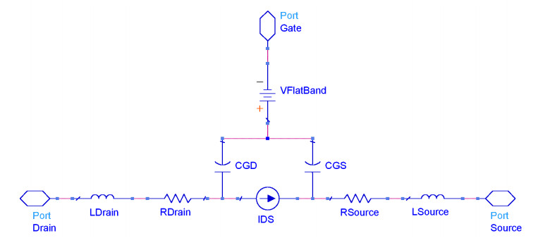
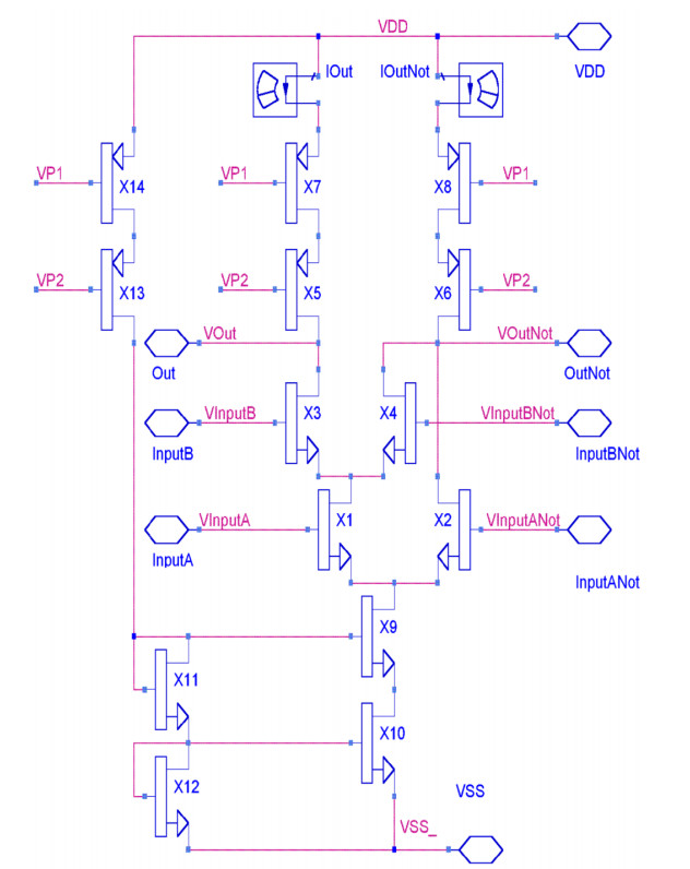
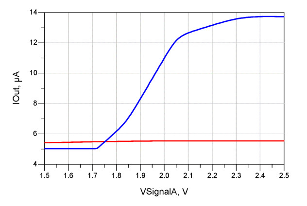
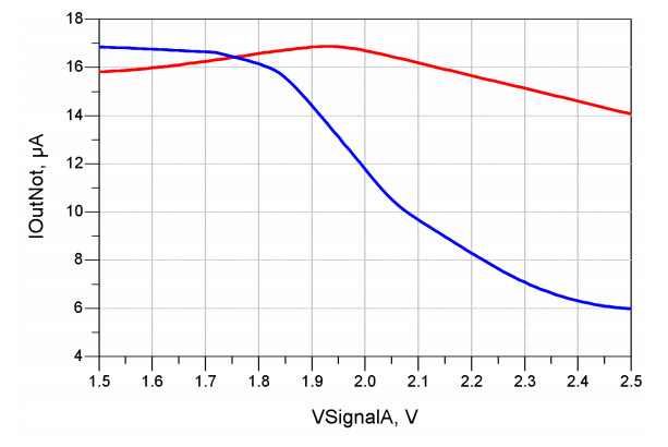
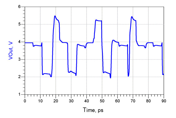
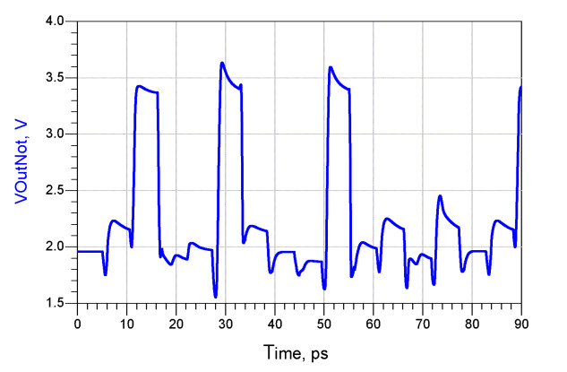
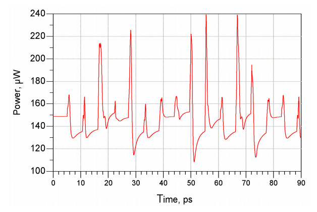
In this letter we present a current mode gate based on differential pair as an application of carbon nanotube field effect transistors (CNTFETs). The proposed circuit has two output logic gates: one is NAND, and the other is AND. To simplify the circuit realization we use all CNTFETs of the same type, all with the same lengths and carbon nanotube symmetry indices (n, m). Complex circuits could be obtained in current mode replicating the differential pair CNTFET along the current path. The proposed procedure allows simulation of transfer characteristics from voltage input to current output but also from voltage input to voltage output. Moreover, we can measure simulated power dissipation and delay times.
Citation: Gennaro Gelao, Roberto Marani, Anna Gina Perri. Analysis and design of current mode logic based on CNTFET[J]. AIMS Materials Science, 2023, 10(6): 965-980. doi: 10.3934/matersci.2023052
In this letter we present a current mode gate based on differential pair as an application of carbon nanotube field effect transistors (CNTFETs). The proposed circuit has two output logic gates: one is NAND, and the other is AND. To simplify the circuit realization we use all CNTFETs of the same type, all with the same lengths and carbon nanotube symmetry indices (n, m). Complex circuits could be obtained in current mode replicating the differential pair CNTFET along the current path. The proposed procedure allows simulation of transfer characteristics from voltage input to current output but also from voltage input to voltage output. Moreover, we can measure simulated power dissipation and delay times.

| [1] |
Marani R, Perri AG (2009) CNTFET modelling for electronic circuit design. ECS Trans 23: 429–437. https://dx.doi.org/10.1149/1.3183748 doi: 10.1149/1.3183748

|
| [2] |
Gelao G, Marani R, Diana R, et al. (2011) A semiempirical SPICE model for n-type conventional CNTFETs. IEEE Trans Nanotechnol 10: 506–512. https://dx.doi.org/10.1109/TNANO.2010.2049499 doi: 10.1109/TNANO.2010.2049499
|
| [3] |
Marani R, Perri AG (2011) A compact, semi-empirical model of carbon nanotube field effect transistors oriented to simulation software. Curr Nanosci 7: 245–253. https://dx.doi.org/10.2174/157341311794653613 doi: 10.2174/157341311794653613
|
| [4] |
Marani R, Perri AG (2012) A DC model of carbon nanotube field effect transistor for CAD applications. Int J Electron 99: 437–444. https://dx.doi.org/10.1080/00207217.2011.629223 doi: 10.1080/00207217.2011.629223
|
| [5] |
Marani R, Gelao G, Perri AG (2012) Comparison of ABM SPICE library with Verilog-A for compact CNTFET model implementation. Curr Nanosci 8: 556–565. https://dx.doi.org/10.2174/157341312801784230 doi: 10.2174/157341312801784230
|
| [6] |
Marani R, Gelao G, Perri AG (2013) Modelling of carbon nanotube field effect transistors oriented to SPICE software for A/D circuit design. Microelectron J 44: 33–38. https://dx.doi.org/10.1016/j.mejo.2011.07.012 doi: 10.1016/j.mejo.2011.07.012
|
| [7] |
Marani R, Perri AG (2016) Analysis of CNTFETs operating in subthreshold region for low power digital applications. ECS J Solid State Sci Technol 5: M1–M4. https://dx.doi.org/10.1149/2.0151602jss doi: 10.1149/2.0151602jss
|
| [8] |
Marani R, Perri AG (2016) A de-embedding procedure to determine the equivalent circuit parameters of RF CNTFETs. ECS J Solid State Sci Technol 5: M31–M34. https://dx.doi.org/10.1149/2.0121605jss doi: 10.1149/2.0121605jss
|
| [9] |
Gelao G, Marani R, Pizzulli L, et al. (2015) A model to improve analysis of CNTFET logic gates in Verilog-A—Part Ⅰ: Static analysis. Curr Nanosci 11: 515–526. https://dx.doi.org/10.2174/1573413711666150320231414 doi: 10.2174/1573413711666150320231414
|
| [10] |
Gelao G, Marani R, Pizzulli L, et al. (2015) A model to improve analysis of CNTFET logic gates in Verilog-A—Part Ⅱ: Dynamic analysis. Curr Nanosci 11: 770–783. https://dx.doi.org/10.2174/1573413711666150624170310 doi: 10.2174/1573413711666150624170310
|
| [11] |
Marani R, Perri AG (2016) A simulation study of analogue and logic circuits with CNTFETs. ECS J Solid State Sci Technol 5: M38–M43. https://dx.doi.org/10.1149/2.0241606jss doi: 10.1149/2.0241606jss
|
| [12] |
Marani R, Perri AG (2016) A comparison of CNTFET models through the design of a SRAM cell. ECS J Solid State Sci Technol 5: M118–M126. https://dx.doi.org/10.1149/2.0161610jss doi: 10.1149/2.0161610jss
|
| [13] |
Marani R, Gelao G, Perri AG (2017) A compact noise model for C-CNTFETs. ECS J Solid State Sci Technol 6: M44–M49. https://dx.doi.org/10.1149/2.0341704jss doi: 10.1149/2.0341704jss
|
| [14] |
Marani R, Perri AG (2017) CNTFET-based design of current mirror in comparison with MOS technology. ECS J Solid State Sci Technol 6: M60–M68. https://dx.doi.org/10.1149/2.0261705jss doi: 10.1149/2.0261705jss
|
| [15] |
Gelao G, Marani R, Perri AG (2018) Effects of temperature in CNTFET-based design of analog circuits. ECS J Solid State Sci Technol 7: M16–M21. https://dx.doi.org/10.1149/2.0031803jss doi: 10.1149/2.0031803jss
|
| [16] |
Gelao G, Marani R, Perri AG (2018) Effects of temperature in CNTFET-based design of digital circuits. ECS J Solid State Sci Technol 7: M41–M48. https://dx.doi.org/10.1149/2.0261803jss doi: 10.1149/2.0261803jss
|
| [17] |
Marani R, Perri AG (2019) A review on the study of temperature effects in the design of A/D circuits based on CNTFET. Curr Nanosci 15: 471–480. https://dx.doi.org/10.2174/1573413714666181009125058 doi: 10.2174/1573413714666181009125058
|
| [18] |
Gelao G, Marani R, Perri AG (2019) A formula to determine energy band gap in semiconducting carbon nanotubes. ECS J Solid State Sci Technol 8: M19–M21. https://dx.doi.org/10.1149/2.0201902jss doi: 10.1149/2.0201902jss
|
| [19] |
Marani R, Perri AG (2020) Techniques to improve the performance in the CNTFET-based analogue circuit design. ECS J Solid State Sci Technol 9: 031001. https://dx.doi.org/10.1149/2162-8777/ab7645 doi: 10.1149/2162-8777/ab7645
|
| [20] |
Marani R, Perri AG (2022) Study of CNTFETs as memory devices. ECS J Solid State Sci Technol 11: 031006. https://dx.doi.org/10.1149/2162-8777/ac5846 doi: 10.1149/2162-8777/ac5846
|
| [21] |
Gelao G, Marani R, Perri AG (2023) Effect of CNT parameter variations on CNTFET amplifier performance. ECS J Solid State Sci Technol 12: 011004. https://dx.doi.org/10.1149/2162-8777/acb1d5 doi: 10.1149/2162-8777/acb1d5
|
| [22] |
Marani R, Perri AG (2023) A technique, based on thevenin equivalent method, to study the noise performance of analog circuits involving both CNTFET and MOS devices. Int J Nanosci Nanotechnol 19: 9–19. https://dx.doi.org/10.22034/ijnn.2023.1988468.2327 doi: 10.22034/ijnn.2023.1988468.2327
|
| [23] | Narud J, Seelbach W, Miller N (1963) Relative merits of current mode logic in microminiaturization. IEEE International Solid-State Circuits Conference, 104–105. |
| [24] | Rashid A (1969) High-speed LSI current-mode-logic arrays for LIMAC. IEEE International Solid-State Circuits Conference, 68–69. |
| [25] |
Raychowdhury A, Mukhopadhyay S, Roy K (2004) A circuit-compatible model of ballistic carbon nanotube field-effect transistors. IEEE T Comput Aid D 23: 1411–1420. https://dx.doi.org/10.1109/TCAD.2004.835135 doi: 10.1109/TCAD.2004.835135
|
| [26] | Pregaldiny F, Lallement C, Kammerer JB (2006) Design-oriented compact models for CNTFETs. International Conference on Design and Test of Integrated Systems in Nanoscale Technology, 34–39. |
| [27] | Datta S (1995) Electronic Transport in Mesoscopic Systems (Cambridge Studies in Semiconductor Physics and Microelectronic Engineering), Cambridge: Cambridge University Press. https://dx.doi.org/10.1017/CBO9780511805776 |
| [28] |
Avouris P, Chen Z, Perebeinos V (2007) Carbon-based electronics. Nature Nanotech 2: 605–615. https://dx.doi.org/10.1038/nnano.2007.300 doi: 10.1038/nnano.2007.300
|
| [29] |
Javey A, Kim H, Brink M, et al. (2002) High-κ dielectrics for advanced carbon-nanotube transistors and logic gates. Nature Mater 1: 241–246. https://dx.doi.org/10.1038/nmat769 doi: 10.1038/nmat769
|
| [30] | Verilog-AMS Language Reference Manual. Available from: https://accellera.org/images/downloads/standards/v-ams/VAMS-LRM-2-4.pdf. |
| [31] |
Lee CS, Pop E, Franklin AD, et al. (2015) A compact virtual-source model for Carbon Nanotube FETs in the sub-10-nm regime—Part Ⅰ: Intrinsic elements. IEEE Trans Electron Devices 62: 3061–3069. https://dx.doi.org/10.1109/TED.2015.2457453 doi: 10.1109/TED.2015.2457453
|
| [32] |
Lee CS, Pop E, Franklin AD, et al. (2015) A compact virtual-source model for Carbon Nanotube FETs in the sub-10-nm regime—Part Ⅱ: Extrinsic elements, performance assessment and design optimization. IEEE Trans Electron Devices 62: 3070–3078. https://dx.doi.org/10.1109/TED.2015.2457424 doi: 10.1109/TED.2015.2457424
|
| [33] |
Marani R, Perri AG (2022) Implementation of noise effects on CNTFET-based NOT gate in Verilog-A. ECS J Solid State Sci Technol 11: 061002. https://dx.doi.org/10.1149/2162-8777/ac7580 doi: 10.1149/2162-8777/ac7580
|
| [34] |
Marani R, Perri AG (2020) Editors' choice—Effects of parasitic elements of interconnection lines in CNT embedded integrated circuits. ECS J Solid State Sci Technol 9: 021004. https://dx.doi.org/10.1149/2162-8777/ab69b2 doi: 10.1149/2162-8777/ab69b2
|
| [35] |
Marani R, Perri AG (2020) Impact of technology on CNTFET-based circuits performance. ECS J Solid State Sci Technol 9: 051001. https://dx.doi.org/10.1149/2162-8777/ab9185 doi: 10.1149/2162-8777/ab9185
|
Figures(15)

Gennaro Gelao, Roberto Marani, Anna Gina Perri. Analysis and design of current mode logic based on CNTFET[J]. AIMS Materials Science, 2023, 10(6): 965-980. doi: 10.3934/matersci.2023052


 DownLoad: