Processing math: 100%
Research article Special Issues

Synergistic design of an integrated pv/distillation solar system based on nanofluid spectral splitting technique

  • Received: 16 January 2021 Accepted: 09 May 2021 Published: 17 May 2021
  • In the present work, an improved hybrid photovoltaic/distillation (PV/D) solar collector with nanofluid-based spectral splitting technique is redesigned by a synergistic design strategy to overcome the flaws of previous experiment system. In such a system, gold nanofluid plays a dual role as a heat absorption medium and a spectral splitting filter to enhance the distillation of water. This system can maximize the utilization of solar energy in whole spectrum, and can obtain electricity and freshwater simultaneously. However, the design of such an integrated hybrid system also become more complicated. Optical and thermal features of the system must be considered carefully and should be synergistically designed in the system. Specifically, an optical simulation is used to improve the configurations of the evaporator and increase the PV efficiency of the system. Another numerical model based on computational fluid dynamics is performed to optimize the layout of moist air circulation and enhance the condensation of vapor in the system. The experimental results confirmed the potential of nanofluid-based spectral splitting technique in solar distillation application. In comparison with the conventional system, the total efficiency of solar energy in the improved system with gold nanoparticles of 3.1 μg/mL, 10.2 μg/mL and 14.1 μg/mL concentration increases by 59.27%, 62.80% and 64.40%, respectively. The water yield per unit area of the improved system with different nanoparticle concentration increases by 35.32%, 37.59% and 42.62%, respectively. These results indicate that the improved system not only can realize the self-sufficiency, but also can carry out a flexible adjustment between PV and desalination units by changing the optical properties of the nanofluid. It can meet a versatile demand of power and heat in more extensive applications.

    Citation: Wei An, Yifan Zhang, Bo Pang, Jun Wu. Synergistic design of an integrated pv/distillation solar system based on nanofluid spectral splitting technique[J]. AIMS Energy, 2021, 9(3): 534-557. doi: 10.3934/energy.2021026

    Related Papers:

    [1] Ibraheem Ahmad Qeays, Syed Mohd. Yahya, M. Saad Bin Arif, Azhar Jamil . Nanofluids application in hybrid Photovoltaic Thermal System for Performance Enhancement: A review. AIMS Energy, 2020, 8(3): 365-393. doi: 10.3934/energy.2020.3.365
    [2] Kaovinath Appalasamy, R Mamat, Sudhakar Kumarasamy . Smart thermal management of photovoltaic systems: Innovative strategies. AIMS Energy, 2025, 13(2): 309-353. doi: 10.3934/energy.2025013
    [3] Sabir Rustemli, Zeki İlcihan, Gökhan Sahin, Wilfried G. J. H. M. van Sark . A novel design and simulation of a mechanical coordinate based photovoltaic solar tracking system. AIMS Energy, 2023, 11(5): 753-773. doi: 10.3934/energy.2023037
    [4] Nadwan Majeed Ali, Handri Ammari . Design of a hybrid wind-solar street lighting system to power LED lights on highway poles. AIMS Energy, 2022, 10(2): 177-190. doi: 10.3934/energy.2022010
    [5] Michael O. Dioha, Atul Kumar . Rooftop solar PV for urban residential buildings of Nigeria: A preliminary attempt towards potential estimation. AIMS Energy, 2018, 6(5): 710-734. doi: 10.3934/energy.2018.5.710
    [6] Fadhil Khadoum Alhousni, Firas Basim Ismail, Paul C. Okonkwo, Hassan Mohamed, Bright O. Okonkwo, Omar A. Al-Shahri . A review of PV solar energy system operations and applications in Dhofar Oman. AIMS Energy, 2022, 10(4): 858-884. doi: 10.3934/energy.2022039
    [7] Imam Abadi, Chairul Imron, Mohammad Musa Bachrowi, Dwi Nur Fitriyanah . Design and implementation of battery charging system on solar tracker based stand alone PV using fuzzy modified particle swarm optimization. AIMS Energy, 2020, 8(1): 142-155. doi: 10.3934/energy.2020.1.142
    [8] Rashmi Murali, Sangeeta Malhotra, Debajit Palit, Krishnapada Sasmal . Socio-technical assessment of solar photovoltaic systems implemented for rural electrification in selected villages of Sundarbans region of India. AIMS Energy, 2015, 3(4): 612-634. doi: 10.3934/energy.2015.4.612
    [9] Jin H. Jo, Kadi Ilves, Tyler Barth, Ellen Leszczynski . Implementation of a large-scale solar photovoltaic system at a higher education institution in Illinois, USA. AIMS Energy, 2017, 5(1): 54-62. doi: 10.3934/energy.2017.1.54
    [10] Humaid Abdullah ALHinai, Azrul Mohd Ariffin, Miszaina Osman . Revolutionizing Oman's energy network with an optimal mixture renewable energy source. AIMS Energy, 2023, 11(4): 628-662. doi: 10.3934/energy.2023032
  • In the present work, an improved hybrid photovoltaic/distillation (PV/D) solar collector with nanofluid-based spectral splitting technique is redesigned by a synergistic design strategy to overcome the flaws of previous experiment system. In such a system, gold nanofluid plays a dual role as a heat absorption medium and a spectral splitting filter to enhance the distillation of water. This system can maximize the utilization of solar energy in whole spectrum, and can obtain electricity and freshwater simultaneously. However, the design of such an integrated hybrid system also become more complicated. Optical and thermal features of the system must be considered carefully and should be synergistically designed in the system. Specifically, an optical simulation is used to improve the configurations of the evaporator and increase the PV efficiency of the system. Another numerical model based on computational fluid dynamics is performed to optimize the layout of moist air circulation and enhance the condensation of vapor in the system. The experimental results confirmed the potential of nanofluid-based spectral splitting technique in solar distillation application. In comparison with the conventional system, the total efficiency of solar energy in the improved system with gold nanoparticles of 3.1 μg/mL, 10.2 μg/mL and 14.1 μg/mL concentration increases by 59.27%, 62.80% and 64.40%, respectively. The water yield per unit area of the improved system with different nanoparticle concentration increases by 35.32%, 37.59% and 42.62%, respectively. These results indicate that the improved system not only can realize the self-sufficiency, but also can carry out a flexible adjustment between PV and desalination units by changing the optical properties of the nanofluid. It can meet a versatile demand of power and heat in more extensive applications.


    In the most recent technological advancements, the creation of high frequency operating multilayer printed circuit boards have received considerable attention. It offers a dependable and economical manufacturing technique that efficiently realizes passive planar components, power buses and high-speed interconnects. Structures are employed in a variety of electronic applications, such as high-speed digital, analogue and microwave circuits. A sizable amount of multilayer PCB technology has been developed for high-speed circuit design for power processing [1]. Additionally, it was developed for mixed-signal devices that can fit onto a small space on PCBs, which often exchange metal traces and planes, as opposed to high-speed PCBs that require numerous layers. However, the signal and power integrity issues continue to be more difficult despite the design advancements in the usage of numerous layers and device placement.

    Present-day mixed-signal systems are particularly susceptible to simultaneous switching noise (SSN) on the signal and ground planes because they combine high-speed CPUs, RF circuits and analogue components onto just one multilayer printed circuit board. The ground and signal layers are affected by the SSN that digital switching components emit. It greatly reduces system performance, which lowers the noise margin and lowers sensitivity. As a result of recent advancements in digital devices' operational frequencies with different data rates, SSN spectral contents now cover a wide frequency range for mixed mode applications [1,2]. Due to continuous increases in data rate and clock frequency, a significant problem of SSN, is becoming more of an issue for higher frequency applications. In high-speed printed circuit boards, a voltage fluctuation known as simultaneous switching noise is an effect of resonance in the cavity mode in signal planes [2,3]. Power integrity and signal integrity are hampered by resonance modes on the ground and power planes. High-speed circuits and PCBs also frequently experience issues with electromagnetic interference. According to studies, signal and power integrity issues have effects on both the temporal and voltage domains. Therefore, it is essential for electronics systems to ensure signal and power integrity. It may reduce the effect of noise [4‒6] by adjusting the time of the system.

    Simultaneous switching noise is reduced by High Impedance Surfaces (HIS), such as Electromagnetic Band Gap (EBG). EBG has been discovered to be useful in many applications, because of its special wave attenuation properties. Periodic patches in the form of mushrooms are present in EBG designs, and the patches are connected to the ground using vias [7]. Wide band gaps for high-speed circuits have been proposed using hybrid EBG structures, which integrate multiple designs [8,9,10,11]. The use of mixed combination EBG structures, which combine two or more structures, have been proposed for high-speed circuits [11,12,13,14]. Electromagnetic bandgap structures are widely used because of their miniature size, which is advantageous for bandgap spectrum enhancement by mitigating their power noise effect at GHz range frequencies. Many planar EBG designs [15,16,17,18,19,20] are used to reduce the effect of electromagnetic compatibility from printed circuit boards. The attenuation reduction in fast speeds design is accomplished via a succession of patches fastened to several types of meander lines and bridges [21,22,23,24,25]. From the published review mentioned above, it is clear that SSN attenuation and band expansion are receiving increased attention.

    The majority of planar EBG structure research that focuses on enlarging the bandgap or the EBG layer is always worked as an outside multilayer by some operation. The ordinary filtering function of the planar EBG used as an internal layer cannot be assured when particular design changes fail to occur. When buried in the stack-up, the EBG layer is frequently sandwiched between two ground plates. The requisite bandgap is not provided by the top cavity or the lower cavity associated with used configuration. The modes of the two solid plates may be observed inside the appropriate bandgap as a result of noise coupling that takes place between the two cavities through the EBG layer gaps. By preventing the resonances of the two solid planes cavities, the filtering capabilities connected to the top and lower cavities can be recovered. A band gap effect can be produced by connecting the two solid ground planes using vias. In order to create a ring that is circular in shape around the vias, the EBG layer separates the patches from the vias [16,17].

    Even though EBG structures are currently in use, they are not appropriate for power noise reduction at the lower frequency limits due to their lower frequency flow, which often uses more from higher frequency ranges. The flow of present EBG structures must be reduced without impacting the suppression in order to bandwidth enhancement encompassing the lower frequency limits. In multilayer PCBs, broad reduction of power/ground noise has been achieved using EBG configurations but not with lower limit of flow. Stepped impedance (SI) structures are the foundation of one of the basic configurations of EBG structures [17,18,19,20]. Stepped impedance EBG structures have been the focus of numerous investigations due to its simple design and broad stopband with significant suppression level. The goal is to decrease flow in lower frequency limits with proper EBG unit cells. The objective of using appropriate EBG cells is to reduce flow in lower frequency limitations.

    In this paper, a rectangular EBG unit cell is designed to broaden the reduction of SSN linking with low flow. It is suggested a stepped impedance (SI) multilayer EBG structure, low pass filters with multiple lines of exceptionally high and low specific impedance will be used by SI. These filters are called stepped-impedance filters, High-Impedance (H-I) filters or Low-Impedance (L-I) filters and are used because they are simpler to design and need less space. The topmost signal layer and internal signal layers of the signal planes in the structure are connected upright by the metal patches to produce a maximum impedance called H-I patch and a minimum impedance is called L-I patch in the suggested multilayer design. The H-I and L-I patches with the SI design are connected through via upright from other layers, the suggested design offers substantial branch inductance in contrast to the planar two-dimensional EBG structure and reference plane. The SSN reduction bandwidth was then improved using rectangular patch design EBG cell size, which resulted in a decrease in flow. Our main idea of this paper is to design a multilayer structure using a step impedance technique, which has advantages of broad stopband, high suppression level and simplified broad connections. If one of the two surfaces is etched appropriately, a series of rectangular patches connected by thin bridges/vias can be produced, altering the resonance behavior of the mentioned perfect cavity. Due to the forced conduction of current through the bridges/vias, the changing geometry has an impact on the electromagnetic field inside the cavity at the resonant frequencies. This effect affects the downshifted resonant frequencies, shown as the operation principle for a suggested design. It is observed that the flow value starts at 817 MHz and that the considerable stopband addition occurs between 817 MHz and 26.32 MHz. This frequency range is suitable for microwave applications including microwave ovens, digital television broadcasting, satellite systems and radar transmitters.

    The following subsections describe design and full wave simulation of the proposed multilayer EBG structure utilizing a wide stopband for SSN mitigation.

    EBG structures have a greater bandgap and demonstrate permeability-negative behavior at frequencies above their resonant frequencies. It is supposed that a parallel plate waveguide has a thinner dielectric layer compared to its width and length. Helmholtz equations are used to calculate resonance frequencies [21,22].

    fTMpq=c2πμr.ϵr(pπ)A2+(qπ)B2 (2.1)

    where 'p' is length of assumed structure, 'q' is width of assumed structure and 'c', 𝜖𝑟 and 𝜇𝑟 are permittivity velocities. In general patch and substrate provide minimum impedance whereas substrate and branch provide maximum impedance. It is possible to determine characteristics impedance by [23],

    Z0=ηdWLC (2.2)

    where, 'W' is patch width, 'd' is the dielectric thickness, 'L' is a patch and other plate inductance. 'C' is a branch and other plate capacitance and '𝜂' is FR4 internal impedance. This establishes a stopband in the desired frequency range.

    flow=12πcμr.ϵrZ0LW (2.3)

    Initial frequency (flow) and higher frequency limit (fhigh) determination is done by the equation (2.3) and (2.4) for mode 1,

    fhigh=12cμr.ϵrZ0W (2.4)

    When the starting low frequency of the bandgap has a mode value of (zero, one), the patch dimensions are calculated [24] using Eq (2.4). The impacts of length and breadth variations, as well as the likelihood of reaching a greater bandgap, are used to determine the branch dimensions.

    The reference plane (without EBG) is more susceptible to being affected by simultaneous switching noise. It is also designed without an EBG reference plane with the same dimensions, for correct comparison of suggested design. Proposed multilayer structure is designed with a stepped impedance method and with a rectangular shape patch. The suggested EBG structure is made of six periodic power plane layers with metal patches connected upright with the other layer patch and there is an alternate complete ground layer. Rectangular shaped designed unit cell with length of the patch is 16 mm and width of patch is 13 mm. Each patch is connected with branch connections at the left and right side, branch length is 2 mm and the branch width is 1 mm in dimensions. The distance between H-I and L-I patches is 0.1 mm and for both H-I patches is 0.4 mm as depicted in Figure 1.

    Figure 1.  Unit cell design with dimensions.

    As shown in Figure 2, the H-I and L-I patches in the various layers are linked to one another by an upright connection of via with a branch made up of small structure on both the sides on the top and inner layers. Additionally, H-I patches are internally connected through via with different distances and layers. An FR-4 epoxy with a loss tangent (𝛿) of 0.02 and a relative permittivity (𝜖𝑟) of 4.4 is used as a dielectric material. Ports are created as shown in Figure 3. The complete suggested multilayer structure with all the layers is in sink as shown in Figure 3. Ground vias are also present in original design but not mentioned in Figure 3 for the clear visualization of design. A common limit is set up to reduce simultaneous switching noise. High-frequency structure simulator (HFSS) by an Analysis System (ANSYS) performs the input-impedance and scattering characteristics as a frequency response [26].

    Figure 2.  Patch connections through vias in stepped impedance technique (Ground via connections as well as ground plane are not shown).
    Figure 3.  Complete periodic structure with vias and all layer connections (ground vias are not shown).

    Planar structure is designed for a better comparison with multilayer structure. For one voltage level, the structure in Figure 3 has a continuous layer, while the EBG designed plane is at another voltage level in two-dimension form. As seen in Figure 11 a, a top view of a 2 X 6 structure is depicted, with the top layer being a periodic structure, or EBG, and the base layer, being a continuous ground plane. The plane of ground and the EBG designed power plane are separated by a dielectric layer. FR-4 epoxy used as a dielectric material. Specially created ports make it simpler to check insertion loss. There are six rectangular patches that are linked together by branches, in a similar manner of proposed multilayer design as shown in Figure 3. The branches add more inductive impact, whereas patches add capacitive impact to the design, causing the stopband to broaden in the scattering parameters. To simulate the scattering parameter, the ANSYS High Frequency Structure Simulator (HFSS) is utilized [26]. The suggested multilayer design transmission coefficient (S21) is shown in Figure 4 and it provides a satisfactory stopband from 817 MHz to 26.32 GHz frequency. It is also checked for comparison of reflection coefficient S11 and S22 of suggested design as in Figure 5. It also shows good agreement of both reflection coefficients.

    Figure 4.  Transmission coefficient(S21) for suggested plane.
    Figure 5.  Comparison of designed EBG reflection coefficients (S11 and S22).

    In these sections, a unit cell simulation in the ANSYS HFSS eigenmode solution is shown for the purpose of conducting a dispersion diagram. The equivalent circuit for 1-D structure is designed for the calculations of dispersion equation with the help of ABCD parameters using the transfer matrix method [27].

    Extraction of the model of an equivalent circuit for the multilayer EBG design is an important step [25]. As depicted in Figure 6, an equivalent circuit is extracted to design a one-dimensional structure. The upright branch can be represented as an inductance via 'Vib' and branch 'Lbr' by combining the inductance of vias, as well as the branch inductance on the topmost and inner layers. The capacitance 'Cr' serves as a representation for the H-I and the associated ground plane. According to Figure 6, the capacitance 'Cr' represents the L-I patch and the ground plane capacitance. The patch has patch inductance 'Lr', divided in two parts with capacitance.

    Figure 6.  Equivalent circuit for the suggested multilayer design.

    Dispersion analysis of the proposed structure using eigenmode and transmission matrix has been used in this work as given in [23]. The one-dimensional periodic single cell, illustrated in Figure 1, is considered for the analysis. A single cell is connected on both sides with branches and vias. The ground vias connections also exist in the work, but are not mention in the calculations. It is assumed a transmission line segment for the mathematical calculations.

    Tunit  cell=[1Zvi01][1Zbr01][coskTjZosinkTjYosinkTcoskT][1Zbr01][1Zvi01] (3.1)

    where, Zvi=jwL, Impedance of branch and via, kT is transmission line segment of phase delay,

    k=2πfμϵ (3.2)

    where µ is permeability and 𝜖 permittivity of dielectric FR4. Zo is impedance and Yo is admittance of assumed segment, w=2πf, where f is frequency.

    The transmission matrix method uses ABCD parameters as in Figure 7, consider finite length transmission line, with input and output terminals in the form of voltage and current. Hence, the relation between input and output terminal and current and voltage vector is given below,

    S21=2A+BZo+CZo+D (3.3)
    Figure 7.  ABCD matrix representation.

    Equation 3.3 is shown scattering parameters in the form of ABCD matrix.

    [VvIv]=Tunitcell[Vv+1Iv+1] (3.4)

    After some calculations obtained equations are,

    [VvIv]=[ABCD][Vv+1Iv+1] (3.5)

    In this case, γ is equal to α+jβ as given in [30],

    [VvIv]=eγt[Vv+1Iv+1] (3.6)

    The final expression is obtained for the dispersion analysis, shown in Figure 8. A dispersion diagram for the equation is almost similar to the original dispersion diagram obtained from eigenmode simulation in the finite element software. The blue dotted plot indicates equation representation and the red solid graph shows the unit cell eigen plot.

    coskT=coskT2πflowZosinkT (3.7)
    Figure 8.  Dispersion diagram of a unit cell and implemented equation.

    System performance can be analyzed using input impedance parameters and S-parameters. The input impedance (Z11) and scattering parameters (S21) in electromagnetic compatibility are necessary components for determining low impedance [28].

    The suggested multilayer EBG plane does pretty well in decreasing SSN at higher frequencies. A lower-frequency threshold, reduction depth and reduction bandwidth are requirements for SSN mitigation. It is demonstrated that noise reduction works well in the MHz to 30 GHz frequency band when utilizing the full wave simulator for scattering parameters. The ground and power plane H-I and L-I patch and via connections of the proposed EBG plane behave like a parallel plate waveguide.

    Comparative simulation results are represented as without EBG solid plane, two-dimensional planar structure and suggested multilayer EBG design. The results of the simulations demonstrate that, as compared to a solid plane and planar structure with a proposed multilayer design (blue solid plot), the bandgap range of 817 MHz to 26.32 GHz is around the 25.50 GHz bandwidth, as shown in Figure 9, and the proposed structure minimizes wideband noise by a -30 dB isolation level. It is observed that, without an EBG reference plane (red color dotted plot) showing a wide stopband in simulation, it only gives a bandgap at lower frequencies and fails to get wide bandgap at higher values. Moreover, planar structure (green dashed plot) shows a 13.56 GHz to 30 GHz bandgap at higher frequencies but it fails to achieve good stopband range at lower frequencies. It is demonstrated that the proposed structure gives a wide band mitigation of SSN about 25.50 GHz bandwidth.

    Figure 9.  Transmission coefficient (S21) comparison between the reference (without EBG) plane, 2D planar design and the proposed bandwidth enhanced multilayer EBG design.

    In order to see how well the planned structure suppresses SSN, the design is essential to look at its signal propagation capabilities [28]. Impact of noise on system performance is depicted in an eye diagram. Signal quality in high-speed designs is visually represented by an eye diagram. MATLAB software [29] is used in this work to model eye diagrams. An eye diagram is used to conduct a signal integrity analysis of the solid board, planar board and proposed multilayer EBG structure. For the procedure for the eye diagram plotting, a touchstone file is imported from the simulator software HFSS. The number of poles is utilized to calculate the transfer function and rotational function for imported data. The spinning object frequency response has been compared to the original data. Finally, the rotational function that applies to the object to a randomly selected 100 Mbps pulse was plotted on an eye diagram using all measurements like time, amplitude and jitter.

    Figure 10, Figure 11 and Figure 12 show the structure and eye diagram of a reference board, planar board and proposed multilayer board respectively. Characteristics of the eye diagrams are obtained in terms of two parameters like time, amplitude. The crucial part for evaluating the quality of an eye pattern is maximum eye opening (MEO), which exhibits noise voltage, and maximum eye width (MEW), which exhibits temporal jitter. The MEO and MEW values for the suggested structure are 1.94 V and 19.61 ns, respectively, as seen in Figure 12b, while the values for the reference plane are 1.03 V and 5.73 ns and for the planar plane are 1.44 V and 9.09 ns, as shown in Figure 10b and Figure 11b. With the suggested structure for MEO, MEW has a concerning high signal to noise ratio (SNR) of 26.99 with comparison without an EBG board. Comparison Table 1 provides improved results for the suggested design.

    Figure 10.  (a) Without EBG multilayer structure (only layer representation). (b) Eye diagram of without EBG multilayer plane.
    Figure 11.  (a) Planar EBG structure. (b) Eye diagram of planar EBG plane.
    Figure 12.  (a) Proposed EBG multilayer structure. (b) Eye diagram of proposed EBG multilayer plane.
    Table 1.  Eye diagram measurement for comparison.
    Eye Measurement and Parameters Reference structure 2-D planar structure Proposed Multilayer EBG
    In terms of amplitude -Eye Height 1.03 V 1.44 V 1.94 V
    In terms of amplitude -Vertical Opening 1.03 V 1.44 V 1.94 V
    In terms of amplitude-SNR 3.84 6.09 26.99
    In terms of time-Eye Width 4.53 ns 8.31 ns 19.61 ns
    In terms of time-Horizontal Opening 5.73 ns 9.09 ns 19.61 ns

     | Show Table
    DownLoad: CSV

    Any hardware design effectiveness can be examined using reflection coefficient and the input impedance parameter. The Z parameter self-impedance (Z11) is used to assess low impedance. The target impedance ought to be lower than a particular impedance for a system to maintain power integrity [25,28,30]. It is necessary to maintain a system impedance below the desired impedance because of resonance modes brought on by cavity effects in the signal plane. In the MHz range, decoupling capacitors are utilized, but at higher frequencies, they are unable to maintain adequate power integrity. In order to control impedance over a greater frequency range by reducing cavity modes, EBG structures are used at higher frequencies. Figure 13 show the input impedance of the solid plane, 2-D planar plane and proposed multilayer structure to explore the effects of cavity mode damping in the proposed EBG design. It is discovered that more cavity modes are suppressed for a larger range of frequencies from lower value GHz to 30 GHz, in the proposed multilayer EBG plane compared to the solid plane and planar plane. The self-impedance is larger in the reference board and planar board because of signal bus resonance, but it is less in the suggested multilayer structure because of a reduction in power bus resonance due to the arrangement and via connections as shown in Figure 13.

    Figure 13.  Comparison of self-impedance of the solid plane, 2-D planar plane and proposed multilayer design.

    There is comparison of published results with the proposed structure. Table 2 compares the proposed multilayer structure to the results that have been published. In Ref. [1], 12.7 mm of unit cell with 19.35 GHz bandgap was employed. Ref. [31] has a 3.9 GHz bandgap and a 15 mm by 15 mm of unit cell. Ref [32] provides 4.3 GHz bandwidth. With a 25.50 GHz bandwidth and a 13 mm X 16 mm patch size, the proposed multilayer structure exhibits good bandwidth enhancement and noise suppression between 817 GHz and 26.32 GHz.

    Table 2.  A proposed bandwidth enhanced multilayer structure comparison with the published references.
    EBG Structure Suppression Depth = -30dB Suppression Depth = -30dB Suppression Depth = -30dB
    Ref. and Patch size in mm Lower frequency in GHz Higher frequency in GHz Bandwidth in GHz
    Ref [1] 12.7 X 12.7 0.65 20 19.35
    Ref [31] 15 X 15 2.2 6.1 3.9
    Ref [32] 15 X 15 2.1 6.4 4.3
    Proposed structure 13 X 16 0.817 26.32 25.50

     | Show Table
    DownLoad: CSV

    This research suggests a proposed multilayer structure to reduce simultaneous switching noise (SSN). It offers adequate wide band SSN suppression from 817 MHz to 26.32 GHz and a suppression bandwidth of 25.50 GHz with the special design technique. Compared to reference plane and two-dimensional planar plane, the proposed design minimizes SSN effectively for the wide range of frequencies, also compared with published research.

    The proposed structure is verified by dispersion analysis using eigenmode and transmission matrix method, which provides good agreement of specified bandgap. The simulation findings demonstrate strong signal and power integrity. Analysis and HFSS simulations were used to design the suggested structure. The results show that specific branches have more inductance which increase system bandwidth. However, by adding EBG structure onto multilayer PCB, signal integrity issues can be reduced.

    The authors declare that they have not used Artificial Intelligence (AI) tools in the creation of this article.

    The authors declare that there are no conflicts of interest in this paper.


    [1] Reif JH, Alhalabi W (2015) Solar-thermal powered desalination: Its significant challenges and potential. Renewable Sustainable Energy Rev 48: 152-165. doi: 10.1016/j.rser.2015.03.065
    [2] Sharon H, Reddy KS (2015) A review of solar energy driven desalination technologies. Renewable Sustainable Energy Rev 41: 1080-1118. doi: 10.1016/j.rser.2014.09.002
    [3] Kumar PV, Kumar A, Prakash O, et al. (2015) Solar stills system design: A review. Renewable Sustainable Energy Rev 51: 153-181. doi: 10.1016/j.rser.2015.04.103
    [4] He T, Yan L (2009) Application of alternative energy integration technology in sea water distillation. Desalination 249: 104-108. doi: 10.1016/j.desal.2008.07.026
    [5] Prakash P, Velmurugan V (2015) Parameters influencing the productivity of solar stills-A review. Renewable Sustainable Energy Rev 49: 585-609. doi: 10.1016/j.rser.2015.04.136
    [6] 
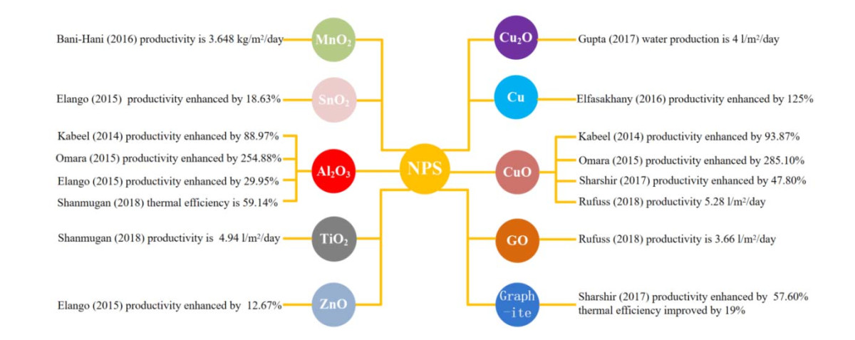
Kabeel AE, Omara ZM, Essa FA (2014) Enhancement of modified solar still integrated with external condenser using nanofluids: An experimental approach. Energy Convers Manage 78: 493-498. doi: 10.1016/j.enconman.2013.11.013
    [7] Omara ZM, Kabeel AE, Younes MM (2014) Enhancing the stepped solar still performance using internal and external reflectors. Energy Convers Manage 78: 876-881. doi: 10.1016/j.enconman.2013.07.092
    [8] Elango T, Kannan A, Murugavel KK (2015) Performance study on single basin single slope solar still with different water nanofluids. Desalination 360: 45-51. doi: 10.1016/j.desal.2015.01.004
    [9] Bani-Hani EH, Borgford C, Khanafer K (2016) Applications of porous materials and nanoparticles in improving solar desalination systems. J Porous Media 19: 993-999. doi: 10.1615/JPorMedia.v19.i11.50
    [10] Elfasakhany A (2016) Performance assessment and productivity of a simple-type solar still integrated with nanocomposite energy storage system. Appl Energy 183: 399-407. doi: 10.1016/j.apenergy.2016.09.002
    [11] Rufuss DDW, Suganthi L, Iniyan S, et al. (2018) Effects of nanoparticle enhanced phase change material (NPCM) on solar still productivity. J Clean Prod 192: 9-29. doi: 10.1016/j.jclepro.2018.04.201
    [12] Shanmugan S, Palani S, Janarthanan B (2018) Productivity enhancement of solar still by PCM and nanoparticles miscellaneous basin absorbing materials. Desalination 433: 186-198. doi: 10.1016/j.desal.2017.11.045
    [13] Sharshir SW, Peng G, Wu L, et al. (2017) Enhancing the solar still performance using nanofluids and glass cover cooling: experimental study. Appl Therm Eng 113: 684-693. doi: 10.1016/j.applthermaleng.2016.11.085
    [14] Gupta B, Kumar A, Baredar PV (2017) Experimental investigation on modified solar still using nanoparticles and water sprinkler attachment. Front Mater 4: 23. doi: 10.3389/fmats.2017.00023
    [15] Kabeel AE, Omara ZM, Essa FA (2014) Improving the performance of solar still by using nanofluids and providing vacuum. Energy Convers Manage 86: 268-274. doi: 10.1016/j.enconman.2014.05.050
    [16] Dev R, Tiwari GN (2010) Characteristic equation of a hybrid (PV-T) active solar still. Desalination 254: 126-137. doi: 10.1016/j.desal.2009.12.004
    [17] Kumar S, Tiwari A (2010) Design, fabrication and performance of a hybrid photovoltaic/thermal (PV/T) active solar still. Energy Convers Manage 51: 1219-1229. doi: 10.1016/j.enconman.2009.12.033
    [18] Yari M, Mazareh AE, Mehr AS (2016) A novel cogeneration system for sustainable water and power production by integration of a solar still and PV module. Desalination 398: 1-11. doi: 10.1016/j.desal.2016.07.004
    [19] Al-Nimr MA, Al-Ammari WA (2016) A novel hybrid PV-distillation system. Sol Energy 135: 874-883. doi: 10.1016/j.solener.2016.06.061
    [20] Manokar AM, Winston DP, Kabeel AE, et al. (2018) Sustainable fresh water and power production by integrating PV panel in inclined solar still. J Clean Prod 172: 2711-2719. doi: 10.1016/j.jclepro.2017.11.140
    [21] An W, Chen L, Liu T, et al. (2018) Enhanced solar distillation by nanofluid-based spectral splitting PV/T technique: Preliminary experiment. Sol Energy 46: 146-156. doi: 10.1016/j.solener.2018.10.029
    [22] Rashidi S, Akar S, Bovand M, et al. (2018) Volume of fluid model to simulate the nanofluid flow and entropy generation in a single slope solar still. Renewable Energy 115: 400-410. doi: 10.1016/j.renene.2017.08.059
    [23] An, W, Li J, Ni J, et al. (2017) Analysis of a temperature dependent optical window for nanofluid-based spectral splitting in PV/T power generation applications. Energy Convers Manage 151: 23-31. doi: 10.1016/j.enconman.2017.08.080
    [24] Ni J, Li J, An W, et al. (2018) Performance analysis of nanofluid-based spectral splitting PV/T system in combined heating and power application. Appl Therm Eng 129: 1160-1170. doi: 10.1016/j.applthermaleng.2017.10.119
    [25] Lee JE, Bera SP, Choi YS, et al. (2017) Size-dependent plasmonic effects of M and M@SiO2 (M = Au or Ag) deposited on TiO2 in photocatalytic oxidation reactions. Appl Catal B- Environ 214: 15-22. doi: 10.1016/j.apcatb.2017.05.025
    [26] Kumar BP, Winston DP, Poinraj P, et al. (2018) Experimental investigation on hybrid PV/T active solar still with effective heating and cover cooling method. Desalination 435: 140-151. doi: 10.1016/j.desal.2017.11.007
    [27] Prakash P, Velmurugan V (2015) Parameters influencing the productivity of solar stills—A review. Renewable Sustainable Energy Rev 49: 585-609. doi: 10.1016/j.rser.2015.04.136
  • Reader Comments
  • © 2021 the Author(s), licensee AIMS Press. This is an open access article distributed under the terms of the Creative Commons Attribution License (http://creativecommons.org/licenses/by/4.0)
通讯作者: 陈斌, bchen63@163.com
  • 1. 

    沈阳化工大学材料科学与工程学院 沈阳 110142

  1. 本站搜索
  2. 百度学术搜索
  3. 万方数据库搜索
  4. CNKI搜索

Metrics

Article views(3176) PDF downloads(132) Cited by(8)

Other Articles By Authors

/

DownLoad:  Full-Size Img  PowerPoint
Return
Return

Catalog