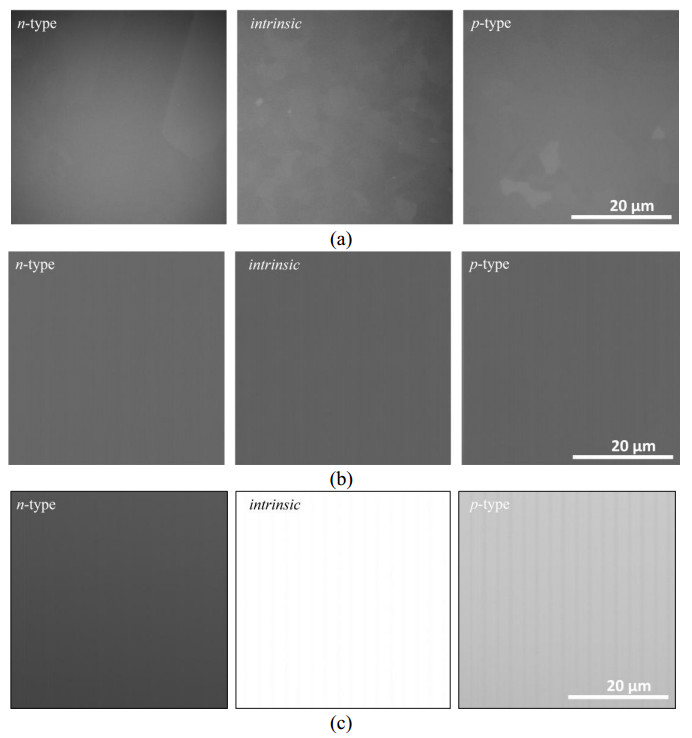
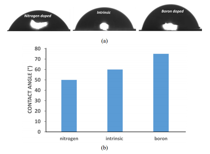
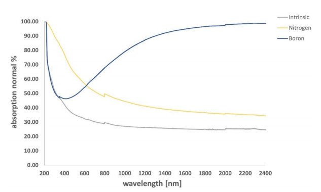
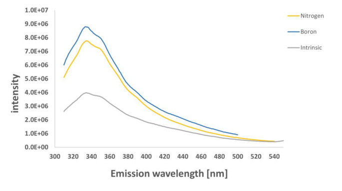
Diamond offers great promise as a solution to some of the limitations of current state of the art semiconductor technologies. Yet, significant challenges associated with the doping process remain a primary impediment to the development of diamond-based electronic devices. At present, it is unclear which simple measurement methods are needed to evaluate the diamond doping process. We propose non-destructive inspection methods for evaluating the polycrystalline chemical vapor deposition (CVD) diamond doping process, by analyzing the wettability, optical absorption, photoluminescence emission spectroscopy and atmospheric scanning electron microscope (Air-SEM) tests. Our results show that the properties of the measured samples are distinctly changed due to the presence of the doping elements, thereby confirming the effectiveness of these non-destructive methods for the diamond production industry.
Citation: Itsh'ak Azoulay, Ory Klonsky, Yaniv Gelbstein, Peter Beker. A study of doped polycrystalline diamond plates by non-destructive methods[J]. AIMS Materials Science, 2023, 10(4): 710-724. doi: 10.3934/matersci.2023039
Diamond offers great promise as a solution to some of the limitations of current state of the art semiconductor technologies. Yet, significant challenges associated with the doping process remain a primary impediment to the development of diamond-based electronic devices. At present, it is unclear which simple measurement methods are needed to evaluate the diamond doping process. We propose non-destructive inspection methods for evaluating the polycrystalline chemical vapor deposition (CVD) diamond doping process, by analyzing the wettability, optical absorption, photoluminescence emission spectroscopy and atmospheric scanning electron microscope (Air-SEM) tests. Our results show that the properties of the measured samples are distinctly changed due to the presence of the doping elements, thereby confirming the effectiveness of these non-destructive methods for the diamond production industry.

| [1] |
Wort CJH, Balmer RS (2008) Diamond as an electronic material. Mater Today 11: 22–28. https://doi.org/10.1016/S1369-7021(07)70349-8 doi: 10.1016/S1369-7021(07)70349-8

|
| [2] | Spear KE, Dismukes JP (1994) Synthetic Diamond: Emerging CVD Science and Technology, New York (N.Y.): Wiley. |
| [3] |
Crawford KG, Maini I, Macdonald DA, et al. (2021) Surface transfer doping of diamond: A review. Prog Surf Sci 96: 100613. https://doi.org/10.1016/j.progsurf.2021.100613 doi: 10.1016/j.progsurf.2021.100613
|
| [4] |
Pinzari F, Ascarelli P, Cappelli E, et al. (2001) Wettability of HF-CVD diamond films. Diam Relat Mater 10: 781–785. https://doi.org/10.1016/S0925-9635(00)00609-9 doi: 10.1016/S0925-9635(00)00609-9
|
| [5] |
Azevedo AF, Baldan MR, Ferreira NG (2013) Doping level influence on chemical surface of diamond electrodes. J Phys Chem Solids 74: 599–604. https://doi.org/10.1016/j.jpcs.2012.12.013 doi: 10.1016/j.jpcs.2012.12.013
|
| [6] |
Li D, Feng X, He J, et al. (2014) Research of surface wettability of plating on the ceramic shell. 2014 15th International Conference on Electronic Packaging Technology, 1208–1211. https://doi.org/10.1109/ICEPT.2014.6922860 doi: 10.1109/ICEPT.2014.6922860
|
| [7] |
Kubiak KJ, Wilson MCT, Mathia TG, et al. (2009) Wettability versus roughness of engineering surfaces. Wear 271: 523–528. https://doi.org/10.1016/j.wear.2010.03.029 doi: 10.1016/j.wear.2010.03.029
|
| [8] |
Frank L, Hovorka M, El-Gomati MM, et al. (2020) Acquisition of the dopant contrast in semiconductors with slow electrons. J Electron Spectrosc 241: 146836. https://doi.org/10.1016/j.elspec.2019.03.004 doi: 10.1016/j.elspec.2019.03.004
|
| [9] |
Alugubelli SR, Fu H, Fu K, et al. (2019) Dopant profiling in p-i-n GaN structures using secondary electrons. J Appl Phys 126: 015704. https://doi.org/10.1063/1.5096273 doi: 10.1063/1.5096273
|
| [10] |
Sealy CP, Castell MR, Wilshaw PR (2000) Mechanism for secondary electron dopant contrast in the SEM. Microscopy 49: 311–321. https://doi.org/10.1093/oxfordjournals.jmicro.a023811 doi: 10.1093/oxfordjournals.jmicro.a023811
|
| [11] |
Choudhary OP, Choudhary P (2017) Scanning Electron Microscope: Advantages and disadvantages in imaging components. Int J Curr Microbiol App Sci 6: 1877–1882. https://doi.org/10.20546/ijcmas.2017.605.207 doi: 10.20546/ijcmas.2017.605.207
|
| [12] |
Bailey GW, Dimlich RVW, McKernan S, et al. (1997) Environmental Scanning Electron Microscopy: -Advantages and disadvantages. Microsc Microanal 3: 381–382. https://doi.org/10.1017/S1431927600008795 doi: 10.1017/S1431927600008795
|
| [13] |
Solomonov I, Talmi-Frank D, Milstein Y, et al. (2014) Introduction of correlative light and airSEM (TM) microscopy imaging for tissue research under ambient conditions. Sci Rep 4: 5987. https://doi.org/10.1038/srep05987 doi: 10.1038/srep05987
|
| [14] | Nebel C (2020) Bulk electronic properties of diamond. arXiv preprint, arXiv: 2005.03884. |
| [15] | Zaitsev AM (2021) Optical Properties of Diamond: A Data Handbook, Berlin, New York: Springer, xvii: 502. |
| [16] |
Walker J (1979) Optical absorption and luminescence in diamond. Rep Prog Phys 42: 1605–1659. https://doi.org/10.1088/0034-4885/42/10/001 doi: 10.1088/0034-4885/42/10/001
|
| [17] |
Mildren RP (2013) Intrinsic Optical Properties of Diamond. Optical Engineering of Diamond 1: 1–34. https://doi.org/10.1002/9783527648603.ch1 doi: 10.1002/9783527648603.ch1
|
| [18] | Egerton RF (2016) Physical Principles of Electron Microscopy: An Introduction to TEM, SEM, and AEM, Springer Cham. https://doi.org/10.1007/978-3-319-39877-8 |
| [19] |
Volotsenko I, Molotskii M, Barkay Z, et al. (2010) Secondary electron doping contrast: Theory based on scanning electron microscope and Kelvin probe force microscopy measurements. J Appl Phys 107: 014510. https://doi.org/10.1063/1.3276090 doi: 10.1063/1.3276090
|
| [20] |
Grunbaum E, Barkay Z, Shapira Y, et al. (2009) Secondary electron emission contrast of quantum wells in GaAs p-i-n junctions. Microsc Microanal 15: 125–129. https://doi.org/10.1017/S1431927609090205 doi: 10.1017/S1431927609090205
|
| [21] |
Li D, Neumann AW (1992) Equation of state for interfacial tensions of solid-liquid systems. Adv Colloid Interface Sci 39: 299–345. https://doi.org/10.1016/0001-8686(92)80064-5 doi: 10.1016/0001-8686(92)80064-5
|
| [22] | Soleimani-gorgani A (2015) Printing on Polymers: Fundamentals and Applications, William Andrew. |
| [23] |
Calvimontes A (2017) The measurement of the surface energy of solids using a laboratory drop tower. npj Microgravity 3: 25. https://doi.org/10.1038/s41526-017-0031-y doi: 10.1038/s41526-017-0031-y
|
| [24] |
Clark CD, Dean PJ, Harris PV, et al. (1964) Intrinsic edge absorption in diamond. Proc R Soc London A-Math Phys Sci 277: 312–329. https://doi.org/10.1098/rspa.1964.0025 doi: 10.1098/rspa.1964.0025
|
| [25] |
Aksenova AS, Altuhov AA, Ryabeva EV, et al. (2017) The investigation of boron-doped diamond absorbance spectrum. J Phys Conf Ser 798: 012149. https://doi.org/10.1088/1742-6596/798/1/012149 doi: 10.1088/1742-6596/798/1/012149
|
| [26] |
Mohapatra DR, Rai P, Misra A, et al. (2007) Photoluminescence study of polycrystalline and single crystal diamond. 2007 International Workshop on Physics of Semiconductor Devices, 891–893. https://doi.org/10.1109/IWPSD.2007.4472665 doi: 10.1109/IWPSD.2007.4472665
|
| [27] |
Achard J, Jacques V, Tallaire A (2020) CVD diamond single crystals with NV centres: a review of material synthesis and technology for quantum sensing applications. J Phys D Appl Phys 53: 313001. https://doi.org/10.1088/1361-6463/ab81d1 doi: 10.1088/1361-6463/ab81d1
|
Figures(5) / Tables(3)

Itsh'ak Azoulay, Ory Klonsky, Yaniv Gelbstein, Peter Beker. A study of doped polycrystalline diamond plates by non-destructive methods[J]. AIMS Materials Science, 2023, 10(4): 710-724. doi: 10.3934/matersci.2023039


 DownLoad: