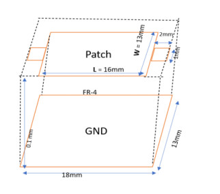
A bandwidth enhanced multilayer Electromagnetic Band Gap (EBG) structure to reduce the simultaneous switching noise (SSN) in high frequency operating circuits, which useful for the satellite communication application, is presented in this paper. A proposed stack structure is mathematically analyzed by the dispersion method and transmission matrix method. Simulation results show good mitigation of SSN in scattering parameters and signal integrity in terms of eye diagrams. We have also checked for power integrity analysis using self-impedance. The proposed structure gives a good SSN suppression at -30 dB from 817 MHz to 26.32 GHz, around 25.50 GHz bandwidth and also reduces the cavity mode resonance within the stopband range. The proposed multilayer structure is compared with planar EBG plane and reference board. It is also compared with published results.
Citation: Manisha R. Bansode, Surendra S. Rathod. A bandwidth enhanced multilayer electromagnetic bandgap structure to reduce the simultaneous switching noise[J]. AIMS Electronics and Electrical Engineering, 2023, 7(4): 406-420. doi: 10.3934/electreng.2023021
A bandwidth enhanced multilayer Electromagnetic Band Gap (EBG) structure to reduce the simultaneous switching noise (SSN) in high frequency operating circuits, which useful for the satellite communication application, is presented in this paper. A proposed stack structure is mathematically analyzed by the dispersion method and transmission matrix method. Simulation results show good mitigation of SSN in scattering parameters and signal integrity in terms of eye diagrams. We have also checked for power integrity analysis using self-impedance. The proposed structure gives a good SSN suppression at -30 dB from 817 MHz to 26.32 GHz, around 25.50 GHz bandwidth and also reduces the cavity mode resonance within the stopband range. The proposed multilayer structure is compared with planar EBG plane and reference board. It is also compared with published results.

| [1] |
Kim M, Koo K, Shim Y, Hwang C, Pak JS, Ahn S, et al. (2012) Vertical Stepped Impedance EBG (VSI-EBG) Structure for Wideband Suppression of Simultaneous Switching Noise in Multilayer PCBs. IEEE T Electromagn Compatibility 55: 307–314. https://doi.org/10.1109/TEMC.2012.2216883 doi: 10.1109/TEMC.2012.2216883

|
| [2] |
Huh SL, Swaminathan M (2012) design technique for embedded electromagnetic band gap structure in load board applications. IEEE T Electromagn Compatibility 54: 443–456. https://doi.org/10.1109/TEMC.2011.2162337 doi: 10.1109/TEMC.2011.2162337
|
| [3] |
Shi LF, Jiang HF (2013) Vertical Cascaded Planar EBG Structure for SSN Suppression. Progress In Electromagnetics Research 142: 423–435. https://doi.org/10.2528/PIER13080107 doi: 10.2528/PIER13080107
|
| [4] | Zhu HR, Mao JF, Li JJ (2013) Signal and power integrity analysis for the novel power plane of EBG structure in high-speed mixed signal systems. IEEE International Wireless Symposium (IWS), 1-4. https://doi.org/10.1109/IEEE-IWS.2013.6616701 |
| [5] |
de Paulis F, Raimondo L, Orlandi (2010) IR-drop analysis and thermal assessment of planar electromagnetic bandgap structures for power integrity applications. IEEE T Adv Packaging 33: 617–622. https://doi.org/10.1109/TADVP.2009.2033572 doi: 10.1109/TADVP.2009.2033572
|
| [6] |
Zhu HR, Sun YF, Huang ZX, Wu XL (2019) A Compact EBG Structure with Etching Spiral Slots for Ultra-Wideband Simultaneous Switching Noise Mitigation in Mixed Signal Systems. IEEE T Comp Pack Man 9: 1559–1567. https://doi.org/10.1109/TCPMT.2018.2888512 doi: 10.1109/TCPMT.2018.2888512
|
| [7] |
Sievenpiper D, Zhang L, Broas RF, Alexopolous NG, Yablonovitch E (1999) High impedance electromagnetic surfaces with a forbidden frequency band. IEEE T Mircow Theory 47: 2059–2073. https://doi.org/10.1109/22.798001 doi: 10.1109/22.798001
|
| [8] |
Kim KH, Schutt-Ainé JE (2008) Analysis and modeling of hybrid planar type electromagnetic-bandgap structures and feasibility study on power distribution network applications. IEEE T Microw Theory 56: 178–186. https://doi.org/10.1109/TMTT.2007.912199 doi: 10.1109/TMTT.2007.912199
|
| [9] |
Wu TL, Wang CC, Lin YH, Wang TK, Chang G (2005) A novel power plane with super-wideband elimination of ground bounce noise on high-speed circuits. IEEE Microwave and Wireless Components Letters 15: 174–176. https://doi.org/10.1109/LMWC.2005.844216 doi: 10.1109/LMWC.2005.844216
|
| [10] |
Karuppiah V, Gurusamy U (2022) Compact EBG structure for ground bounce noise suppression in high-speed digital systems. AIMS Electronics and Electrical Engineering 6: 124–143. https://doi.org/10.3934/electreng.2022008 doi: 10.3934/electreng.2022008
|
| [11] |
Shi LF, Sun ZM, Liu GX, Chen S (2018) Hybrid-Embedded EBG Structure for Ultrawideband Suppression of SSN. IEEE T Electromagn Compatibility 60: 747–753. https://doi.org/10.1109/TEMC.2017.2743039 doi: 10.1109/TEMC.2017.2743039
|
| [12] |
Shi LF, Li KJ, Hu HQ, Chen S (2016) Novel L-EBG Embedded structure for the Suppression of SSN. IEEE T Electromagn Compatibility 58: 241–248. https://doi.org/10.1109/TEMC.2015.2505736 doi: 10.1109/TEMC.2015.2505736
|
| [13] | Paulis FD, Orlandi A, Raimondo L, Antonini G (2009) Fundamental mechanisms of coupling between planar electromagnetic bandgap structures and interconnects in high-speed digital circuits. Part I – Microstrip lines. Proc. EMC European Workshop, 1-4. https://doi.org/10.1109/EMCEUROPE.2009.5189701 |
| [14] |
Shahparnia S, Ramahi OM (2005) Miniaturized electromagnetic bandgap structures for broadband switching noise suppression in PCBs. Electron Lett 41: 519–520. https://doi.org/10.1049/el:20050445 doi: 10.1049/el:20050445
|
| [15] |
Bansode MR, Rathod SS (2005) Compact Planar Electromagnetic Bandgap Structure for Signal and Power Integrity Improvement in High-speed Circuits. Progress In Electromagnetics Research M 114: 233–243. http://dx.doi.org/10.2528/PIERM22102205 doi: 10.2528/PIERM22102205
|
| [16] |
Fan J, Ye X, Kim J, Archambeault B, Orlandi A (2010) Signal Integrity Design for High-Speed Digital Circuits: Progress and Directions. IEEE T Electromagn Compatibility 52: 392–400. https://doi.org/10.1109/TEMC.2010.2045381 doi: 10.1109/TEMC.2010.2045381
|
| [17] |
Wu TL, Fan J, de Paulis F, Wang CD, Scogna AC, Orlandi A (2010) Mitigation of Noise Coupling in Multilayer High-Speed PCB: State of the Art Modeling Methodology and EBG Technology. IEEE T Commun 93: 1678–1689. https://doi.org/10.1587/transcom.E93.B.1678 doi: 10.1587/transcom.E93.B.1678
|
| [18] |
Toyota Y, Engin AE, Kim TH, Swaminathan M (2006) Stopband Analysis Using Dispersion Diagram for Two-Dimensional Electromagnetic Bandgap Structures in Printed Circuit Boards. IEEE Microw Wireless Comp Lett 16: 645–647. https://doi.org/10.1109/LMWC.2006.885587 doi: 10.1109/LMWC.2006.885587
|
| [19] |
Kim M, Kim S, Bae B, Cho J, Kim J, Kim J, et al. (2013) Application of VSI-EBG Structure to High-Speed Differential Signals for Wideband Suppression of Common Mode Noise. ETRI J 35: 827–637. http://dx.doi.org/10.4218/etrij.13.0112.0875 doi: 10.4218/etrij.13.0112.0875
|
| [20] |
Keshwani VR, Bhavarthe PP, Rathod SS (2021) Eight shape Electromagnetic Band Gap structure for bandwidth improvement of wearable antenna. Progress In Electromagnetics Research C 116: 37–49. http://dx.doi.org/10.2528/PIERC21070603 doi: 10.2528/PIERC21070603
|
| [21] |
de Paulis F, Orlandi A (2012) Accurate and efficient analysis of planar electromagnetic band-gap structures for power bus noise mitigation in the GHz band. Progress In Electromagnetics Research B 37: 59–80. http://dx.doi.org/10.2528/PIERB11100402 doi: 10.2528/PIERB11100402
|
| [22] | de Paulis F, Orlandi A (2006) A novel synthesis method for designing electromagnetic bandgap (EBG) structures in packaged mixed signal systems. Proc 56th Electron Compon Technol Conf 1645–1651. https://doi.org/10.1109/ECTC.2006.1645878 |
| [23] | Choi J, Govind V, Swaminathan M (2004) A Novel Electromagnetic Bandgap (EBG) Structure for Mixed-Signal System Applications. IEEE Radio and Wireless Conference 243-246. https://doi.org/10.1109/RAWCON.2004.1389120 |
| [24] |
Lu H, Zhao J, Yu Z (2012) Design and Analysis of a Novel Electromagnetic Bandgap Structure For Suppressing Simultaneous Switching Noise. Progress In Electromagnetics Research C 30: 81–91. https://doi.org/10.2528/PIERC12042709 doi: 10.2528/PIERC12042709
|
| [25] | Bansode MR, Dahatonde R, Rathod SS (2021) Simultaneous Switching Noise Reduction in High-Speed Circuits. IEEE International Conference on Communication information and Computing Technology (ICCICT) 1–4. https://doi.org/10.1109/ICCICT50803.2021.9510097 |
| [26] | High Frequency Structure Simulator. Available from: http://www.ansoft.com. |
| [27] | Pozar M (2013) Microwave Engineering, 3rd ed. New York, NY, USA: Wiley. |
| [28] | Orlandi A, Archambeault B, de Paulis F, Connor S (2017) Impact of Planar EBGs on Signal Integrity in High-Speed Digital Boards. https://doi.org/10.1002/9781119281559.ch3 |
| [29] | The MathWorks, Inc. (2022) MATLAB version: 9.13.0 (R2022b). Accessed: January 01, 2023. Available from: https://www.mathworks.com. |
| [30] | Bansode MR, Rathod SS (2023) Enhanced Signal and Power Integrity using Novel Planar EBG design. 2023 Joint Asia-Pacific International Symposium on Electromagnetic Compatibility and International Conference on Electro Magnetic Interference Compatibility (APEMC/INCEMIC). https://doi.org/10.1109/APEMC57782.2023.10217404 |
| [31] |
Kim M, Ahn S (2013) A Compact and Multi-Stack Electromagnetic Bandgap Structure for Gigahertz Noise Suppression in Multilayer Printed Circuit Boards. Appl Sci 7: 804. https://doi.org/10.3390/app7080804 doi: 10.3390/app7080804
|
| [32] | Kim M (2016) Multi-stack Technique for a Compact and Wideband EBG Structure in High-Speed Multilayer Printed Circuit Boards. ETRI Journals 38: 903-910. |


Figures(13) / Tables(2)

Manisha R. Bansode, Surendra S. Rathod. A bandwidth enhanced multilayer electromagnetic bandgap structure to reduce the simultaneous switching noise[J]. AIMS Electronics and Electrical Engineering, 2023, 7(4): 406-420. doi: 10.3934/electreng.2023021


 DownLoad: