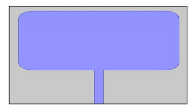
A dual-band google lens logo-based patch antenna with defected ground structure was designed at 5.3 GHz for wireless applications and 7.4 GHz for wi-fi application. The designed antenna consists of a rounded rectangular patch antenna with a partial ground structure fed by a 50 Ω microstrip line. A google lens shaped logo is subtracted from the rounded rectangular patch and some regular polygon shaped slots are subtracted from the ground plane to obtain good dual-band characteristics and better results in terms of gain, VSWR, and return loss. The proposed antenna has a measurement of 20 × 20 × 1.6 mm3 and provides wide impedance bandwidths of 0.23 GHz (5.17‒5.40 GHz) and 0.16 GHz (7.33–7.49 GHz) at center frequencies of 5.3 GHz and 7.4 GHz, respectively. The antenna was designed and simulated using an ANSYS Electronics Desktop. Fabrication of the antenna was obtained using chemical etching and the results were measured by using an MS2037C Anritsu combinational analyzer. The return loss characteristics for dual bands are -20.56 dB at 5.3 GHz and -19.17 dB at 7.4 GHz, respectively, with a VSWR < 2 at both the frequencies and a 4 dB gain is obtained.
Citation: M. Naveen Kumar, M. Venkata Narayana, Govardhani Immadi, P. Satyanarayana, Ambati Navya. Analysis of a low-profile, dual band patch antenna for wireless applications[J]. AIMS Electronics and Electrical Engineering, 2023, 7(2): 171-186. doi: 10.3934/electreng.2023010
A dual-band google lens logo-based patch antenna with defected ground structure was designed at 5.3 GHz for wireless applications and 7.4 GHz for wi-fi application. The designed antenna consists of a rounded rectangular patch antenna with a partial ground structure fed by a 50 Ω microstrip line. A google lens shaped logo is subtracted from the rounded rectangular patch and some regular polygon shaped slots are subtracted from the ground plane to obtain good dual-band characteristics and better results in terms of gain, VSWR, and return loss. The proposed antenna has a measurement of 20 × 20 × 1.6 mm3 and provides wide impedance bandwidths of 0.23 GHz (5.17‒5.40 GHz) and 0.16 GHz (7.33–7.49 GHz) at center frequencies of 5.3 GHz and 7.4 GHz, respectively. The antenna was designed and simulated using an ANSYS Electronics Desktop. Fabrication of the antenna was obtained using chemical etching and the results were measured by using an MS2037C Anritsu combinational analyzer. The return loss characteristics for dual bands are -20.56 dB at 5.3 GHz and -19.17 dB at 7.4 GHz, respectively, with a VSWR < 2 at both the frequencies and a 4 dB gain is obtained.

| [1] |
Yoo JU, Son HW (2020) A simple compact wideband microstrip antenna consisting of three staggered patches. IEEE Antenn Wirel Pr 19: 2038‒2042. https://doi.org/10.1109/LAWP.2020.3021491 doi: 10.1109/LAWP.2020.3021491

|
| [2] | Babu MR, Venkatachari D, Yogitha K, Sri KP, Jagadeesh K, Lokesh M (2020) A Low-Profile Pentagon Inscribed in Circle Shaped Wide Band Antenna Design for C-Band Applications. 2020 IEEE Bangalore Humanitarian Technology Conference (B-HTC), 1‒4. IEEE. |
| [3] | Chen S, Jiang Y, Cao W (2020) A Compact Ultra-Wideband Microstrip patch Antenna for 5G and WLAN. 2020 IEEE 3rd International Conference on Electronic Information and Communication Technology (ICEICT), 601‒603. IEEE. https://doi.org/10.1109/ICEICT51264.2020.9334347 |
| [4] | Kumar G, Grover K, Kulshrestha S (2019) A Compact Microstrip CP Antenna Using Slots and Defected Ground Structure (DGS). 2019 IEEE Indian Conference on Antennas and Propogation (InCAP), 1‒4. IEEE. https://doi.org/10.1109/InCAP47789.2019.9134558 |
| [5] | Patanvariya DG, Kola KS, Chatterjee A (2019) A Circularly-polarized Linear Array of Maple-leaf shaped Antennas for C-band Applications. 2019 10th International Conference on Computing, Communication and Networking Technologies (ICCCNT), 1‒5. IEEE. https://doi.org/10.1109/ICCCNT45670.2019.8944595 |
| [6] | Mahatmanto BP, Apriono C (2020) High Gain 4×4 Microstrip Rectangular Patch Array Antenna for C-Band Satellite Applications. 2020 FORTEI-International Conference on Electrical Engineering (FORTEI-ICEE), 125‒129. IEEE. https://doi.org/10.1109/FORTEI-ICEE50915.2020.9249810 |
| [7] | Maddio S, Pelosi G, Selleri S (2020) A Tri-Band Circularly Polarized Patch Antenna for WiFi Applications in S-and C-band. 2020 IEEE International Symposium on Antennas and Propagation and North American Radio Science Meeting, 1963‒1964. IEEE. https://doi.org/10.1109/IEEECONF35879.2020.9330117 |
| [8] | Srivastava S, Singh AK (2019) Design of Tri-band L Shaped Parasitic Patch Antenna. 2019 URSI Asia-Pacific Radio Science Conference (AP-RASC), 1‒4. IEEE. https://doi.org/10.23919/URSIAP-RASC.2019.8738672 |
| [9] | Abdi M, Aguili T (2019) Design of a Compact Multilayered Aperture Coupled Microstrip Antenna for Automotive Range Radar Application. 2019 IEEE 19th Mediterranean Microwave Symposium (MMS), 1‒4. IEEE. https://doi.org/10.1109/MMS48040.2019.9157286 |
| [10] |
Xu J, Hong W, Jiang ZH, Zhang H (2018) Wideband, low-profile patch array antenna with corporate stacked microstrip and substrate integrated waveguide feeding structure. IEEE T Antenn Propag 67: 1368‒1373. https://doi.org/10.1109/TAP.2018.2883561 doi: 10.1109/TAP.2018.2883561
|
| [11] | Patanvariya DG, Chatterjee A (2020) A Compact Triple-Band Circularly Polarized Slot Antenna for MIMO System. 2020 International Symposium on Antennas & Propagation (APSYM), 54‒57. IEEE. https://doi.org/10.1109/APSYM50265.2020.9350733 |
| [12] | Chen WS, Lin YC, Huang KH (2020) Design of 8-port Cross-Slot Antennas for WRC 5G C-Band MIMO Access Point Applications. 2020 International Workshop on Electromagnetics: Applications and Student Innovation Competition (iWEM), 1‒2. IEEE. https://doi.org/10.1109/iWEM49354.2020.9237426 |
| [13] | Sara S, Abdenacer ES (2019) Novel dual-band dipole antenna integrated with EBG electromagnetic bandgap structures dedicated to mobile communications. 2019 International Conference on Wireless Technologies, Embedded and Intelligent Systems (WITS), 1‒5. IEEE. https://doi.org/10.1109/WITS.2019.8723660 |
| [14] | Sokunbi O, Gaya S, Hamza A, Sheikh SI, Attia H (2020) Enhanced Isolation of MIMO Slot Antenna Array Employing Modified EBG Structure and Rake-Shaped Slots. 2020 IEEE International Symposium on Antennas and Propagation and North American Radio Science Meeting, 1969‒1970. IEEE. https://doi.org/10.1109/IEEECONF35879.2020.9329691 |
| [15] |
Sharma GK, Sharma N (2013) Improving the Performance Parameters of Microstrip Patch antenna by using EBG substrate. IJRET: International Journal of Research in Engineering and Technology 2: 111‒115. https://doi.org/10.15623/ijret.2013.0212019 doi: 10.15623/ijret.2013.0212019
|
| [16] |
Ghouz HHM, Sree MFA, Ibrahim MA (2020) Novel wideband microstrip monopole antenna designs for WiFi/LTE/WiMax devices. IEEE Access 8: 9532‒9539. https://doi.org/10.1109/ACCESS.2019.2963644 doi: 10.1109/ACCESS.2019.2963644
|
| [17] |
Palandoken M (2017) Dual broadband antenna with compact double ring radiators for IEEE 802.11 ac/b/g/n WLAN communication applications. Turk J Electr Eng Comput Sci 25: 1325–1333. https://doi.org/10.3906/elk-1507-121 doi: 10.3906/elk-1507-121
|
| [18] |
Chu HB, Shirai H (2018) A compact metamaterial quad-band antenna based on asymmetric E-CRLH unit cells. PIER C 81: 171–179. https://doi.org/10.2528/PIERC17111605 doi: 10.2528/PIERC17111605
|
| [19] |
Chouhan S, Panda DK, Kushwah VS, Singhal S (2019) Spider-shaped fractal MIMO antenna for WLAN/WiMAX/WiFi/Bluetooth/C-band applications. AEU Int J Electron Commun 110: 152871. https://doi.org/10.1016/j.aeue.2019.152871 doi: 10.1016/j.aeue.2019.152871
|
| [20] |
Ali WAE, Ashraf MI, Salamin MA (2021) A dual-mode double-sided 4×4 MIMO slot antenna with distinct isolation for WLAN/WiMAX applications. Microsyst Technol 27: 967–983. https://doi.org/10.1007/s00542-020-04984-6 doi: 10.1007/s00542-020-04984-6
|
| [21] |
Altaf A, Seo M (2020) Dual-Band Circularly Polarized Dielectric Resonator Antenna for WLAN and WiMAX Applications. Sensors 20: 1137. https://doi.org/10.3390/s20041137 doi: 10.3390/s20041137
|
| [22] |
Liu S, Wu W, Fang DG (2015) Single-Feed Dual-Layer Dual-Band E-Shaped and U-Slot Patch Antenna for Wireless Communication Application. IEEE Antenn Wirel Pr 15: 468–471. https://doi.org/10.1109/LAWP.2015.2453329 doi: 10.1109/LAWP.2015.2453329
|
| [23] |
Benkhadda O, Ahmad S, Saih M, Chaji K, Reha A, Ghaffar A, et al. (2022) Compact Broadband Antenna with Vicsek Fractal Slots for WLAN and WiMAX Applications. Appl Sci 12: 1142. https://doi.org/10.3390/app12031142 doi: 10.3390/app12031142
|
| [24] |
Kumar A, Raghavan S (2018) Planar Cavity-Backed Self-Diplexing Antenna Using Two-Layered Structure. Progress In Electromagnetics Research Letters 76: 91‒96. https://doi.org/10.2528/PIERL18031605 doi: 10.2528/PIERL18031605
|
| [25] |
Kumar A, Imaculate Rosaline S (2021) Hybrid half-mode SIW cavity-backed diplex antenna for on-body transceiver applications. Appl Phys A 127: 1‒7. https://doi.org/10.1007/s00339-021-04978-9 doi: 10.1007/s00339-021-04978-9
|
| [26] |
Kumar A, Chaturvedi D, Raghavan S (2019) Design and experimental verification of dual-Fed, self-diplexed cavity-backed slot antenna using HMSIW technique. IET Microw Antennas Propag 13: 380‒385. https://doi.org/10.1049/iet-map.2018.5327 doi: 10.1049/iet-map.2018.5327
|
| [27] |
Saravanakumar M, Kumar A, Raghawan S (2019) Substrate Integrated Waveguide-fed Wideband Circularly Polarised Antenna with Parasitic Patches. Defence Sci J 69. https://doi.org/10.14429/dsj.69.13049 doi: 10.14429/dsj.69.13049
|
| [28] | Kumar A, Chaturvedi D, Raghavan S (2019) Dual-Band, Dual-Fed Self-Diplexing Antenna. 2019 13th European Conference on Antennas and Propagation (EuCAP), 1‒5. IEEE. |
| [29] | Imamdi G, Narayana MV, Navya A, Roja A (2018) Reflector array antenna design at millimetric band for on the move applications. ARPN Journal of Engineering and Applied Sciences 13: 352‒359. |
| [30] |
Govardhani I, Narayana MV, Navya A, Venkatesh A, Spurjeon SC, Venkat SS, et al. (2017) Design of high directional crossed dipole antenna with metallic sheets for UHF and VHF applications. International Journal of Engineering & Technology 7: 42‒50. https://doi.org/10.14419/ijet.v7i1.5.9120 doi: 10.14419/ijet.v7i1.5.9120
|
| [31] |
Narayana MV, Immadi G, Navya A, Anirudh D, Naveen K, Sriram M (2020) A Non- Foster Elemental Triangular Shaped Patch Antenna for Fm Applications. JCR 7: 468‒470. https://doi.org/10.31838/jcr.07.13.82 doi: 10.31838/jcr.07.13.82
|
| [32] |
Immadi G, Narayana MV, Navya A, Anudeep Varma C, Reddy A, Manisai Deepika A, et al. (2020) Analysis of substrate integrated frequency selective surface antenna for IOT applications. Indonesian Journal of Electrical Engineering and Computer Science 18: 875–888. https://doi.org/10.11591/ijeecs.v18.i2.pp875-881 doi: 10.11591/ijeecs.v18.i2.pp875-881
|


Figures(15) / Tables(2)

M. Naveen Kumar, M. Venkata Narayana, Govardhani Immadi, P. Satyanarayana, Ambati Navya. Analysis of a low-profile, dual band patch antenna for wireless applications[J]. AIMS Electronics and Electrical Engineering, 2023, 7(2): 171-186. doi: 10.3934/electreng.2023010


 DownLoad: