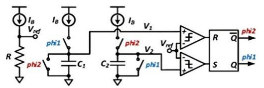
High precision oscillators became a significant call for both designer and testing engineers. Modern vibrators are being utilized in a variety of circuits, and accessibility to a wide range of frequencies is of the utmost importance in all research establishments. To produce various frequencies, utilizing a single gadget is very challenging for the designers. This article aims to provide the low frequency (RC) oscillator and high frequency (LC) oscillators with various output frequencies on a single chip. The use of both oscillators is necessary due to the fact that there are currently no such devices on the market, which makes it necessary to avoid using bulky recurrence generator hardware in order to facilitate rapid exploration and plausibility research. Here, a RC oscillator with high current accuracy and a LC oscillator with low force have been used to design a voltage controlled oscillator (VCO) IC by utilizing the Cadence 45 nm technology. This particular VCO IC is able to obtain two different frequencies with reasonable precision. Further, execution is completed by utilizing exclusive requirement inconsistent message format designing. This proposed work can be used at both audio frequency and radio frequency ranges from megahertz (MHz) to gigahertz (GHz).
Citation: K. Madhava Rao, B. Karthik Reddy, C. Rameshkumar Reddy, K. Charan Kumar, Jakka Yeshwanth Reddy. Implementation of on-chip high precision oscillators with RC and LC using digital compensation technique[J]. AIMS Electronics and Electrical Engineering, 2022, 6(2): 188-197. doi: 10.3934/electreng.2022012
High precision oscillators became a significant call for both designer and testing engineers. Modern vibrators are being utilized in a variety of circuits, and accessibility to a wide range of frequencies is of the utmost importance in all research establishments. To produce various frequencies, utilizing a single gadget is very challenging for the designers. This article aims to provide the low frequency (RC) oscillator and high frequency (LC) oscillators with various output frequencies on a single chip. The use of both oscillators is necessary due to the fact that there are currently no such devices on the market, which makes it necessary to avoid using bulky recurrence generator hardware in order to facilitate rapid exploration and plausibility research. Here, a RC oscillator with high current accuracy and a LC oscillator with low force have been used to design a voltage controlled oscillator (VCO) IC by utilizing the Cadence 45 nm technology. This particular VCO IC is able to obtain two different frequencies with reasonable precision. Further, execution is completed by utilizing exclusive requirement inconsistent message format designing. This proposed work can be used at both audio frequency and radio frequency ranges from megahertz (MHz) to gigahertz (GHz).

| [1] |
Karuppanan P, Ghosh SR, Khan K, et al. (2017) A Fully Differential Operational Amplifier with Slew Rate Enhancer and Adaptive Bias for Ultra-Low Power. J Low Power Electron 13: 67-75. https://doi.org/10.1166/jolpe.2017.1467 doi: 10.1166/jolpe.2017.1467

|
| [2] |
Paidimarri A, Griffith D, Wang A, et al. (2013) A 120 nW 18.5 kHz RC oscillator with comparator offset cancellation for ±0.25% temperature stability. Proc IEEE Int Solid-State Circuits Conf Dig Tech Papers, 184-185. https://doi.org/10.1109/ISSCC.2013.6487692 doi: 10.1109/ISSCC.2013.6487692
|
| [3] |
Zito D, Pepe D, Fonte A (2012) 13 GHz CMOS active inductor LC VCO. IEEE Microw Wireless Compon Lett 22: 138-140. https://doi.org/10.1109/LMWC.2012.2183633 doi: 10.1109/LMWC.2012.2183633
|
| [4] |
Lee S, Nguyen CTC (2004) Phase noise amplitude dependence in self limiting wine-glass disk oscillators. Solid State Sens. Solid State Sensor, Actuator, and Microsystems Workshop, 33-36. https://doi.org/10.31438/trf.hh2004.8 doi: 10.31438/trf.hh2004.8
|
| [5] |
Li G, Afshari E (2011) A distributed dual-band LC oscillator based on mode switching. IEEE T Microw Theory 59: 99-107. https://doi.org/10.1109/TMTT.2010.2091203 doi: 10.1109/TMTT.2010.2091203
|
| [6] |
Liu SL, Chen KH, Chin A (2012) A dual-resonant mode 10/22-GHz VCO with a novel inductive switching approach. IEEE Microw Wireless Compon Lett 60: 2165-2177. https://doi.org/10.1109/TMTT.2012.2195674 doi: 10.1109/TMTT.2012.2195674
|
| [7] | Lee L, George A, Je M (2016) A 1.4 V 10.5 MHz swing-boosted differential relaxation oscillator with 162.1 dBc/Hz FOM and 9.86 psrms period jitter in 0.18 μm CMOS. Proc IEEE Int Solid-State Circuits Conf Dig Tech Papers, 106-108. https://doi.org/10.1109/ISSCC.2016.7417929 |
| [8] | Perrott MH, Salvia JC, Lee FS, et al. (2013) A temperature-to-digital converter for a MEMS-based programmable oscillator with < ±0.5-ppm frequency stability and < 1-ps integrated Jitter. IEEE J Solid-St Circ 48: 276-291. https://doi.org/10.1109/JSSC.2012.2218711 |
| [9] | van Beek JTM, Puers R (2011) A review of MEMS oscillators for frequency reference and timing applications. J Micromech. Microeng 22: 013001. https://doi.org/10.1088/0960-1317/22/1/013001 |
| [10] | Majjad H, Coudevylle JR, Basrour S, et al. (2001) Modeling and characterization of Lamé-mode microresonators realized by UV-LIGA. In Transducers '01 Eurosensors XV, 300-303. https://doi.org/10.1007/978-3-642-59497-7_71 |
| [11] | Swetha Praharsha G, Ommi VS, Raj T, et al. (2022) Design and Analysis of Bulk-Driven Linear Voltage-Controlled Oscillator. Recent Trends in Electronics and Communication, 335-344. https://doi.org/10.1007/978-981-16-2761-3_31 |
| [12] | Cao Y, Leroux P, De Cock W, et al. (2013) A 63,000 Q-factor relaxation oscillator with switched-capacitor integrated error feedback. Proc IEEE Int Solid-state Circuits Conf Dig Tech Papers, 186-187. https://doi.org/10.1109/ISSCC.2013.6487693 |
| [13] | Satoh Y, Kobayashi H, Miyaba T, et al. (2014) A 2.9 mW, ±85 ppm accuracy reference clock generator based on RC oscillator with on-chip temperature calibration. Proc Dig Symp VLSI Circuits, 1-2. https://doi.org/10.1109/VLSIC.2014.6858450 |
| [14] |
Yun SJ, Lee HD, Kim KD, et al. (2010) A widetuning dualband transformer-based complementary VCO. IEEE Microw Wireless Compon Lett 20: 340-342. https://doi.org/10.1109/LMWC.2010.2047524 doi: 10.1109/LMWC.2010.2047524
|


Figures(12) / Tables(2)

K. Madhava Rao, B. Karthik Reddy, C. Rameshkumar Reddy, K. Charan Kumar, Jakka Yeshwanth Reddy. Implementation of on-chip high precision oscillators with RC and LC using digital compensation technique[J]. AIMS Electronics and Electrical Engineering, 2022, 6(2): 188-197. doi: 10.3934/electreng.2022012


 DownLoad: