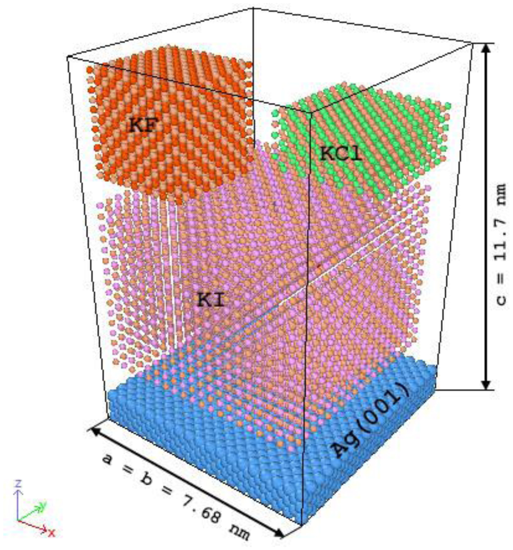
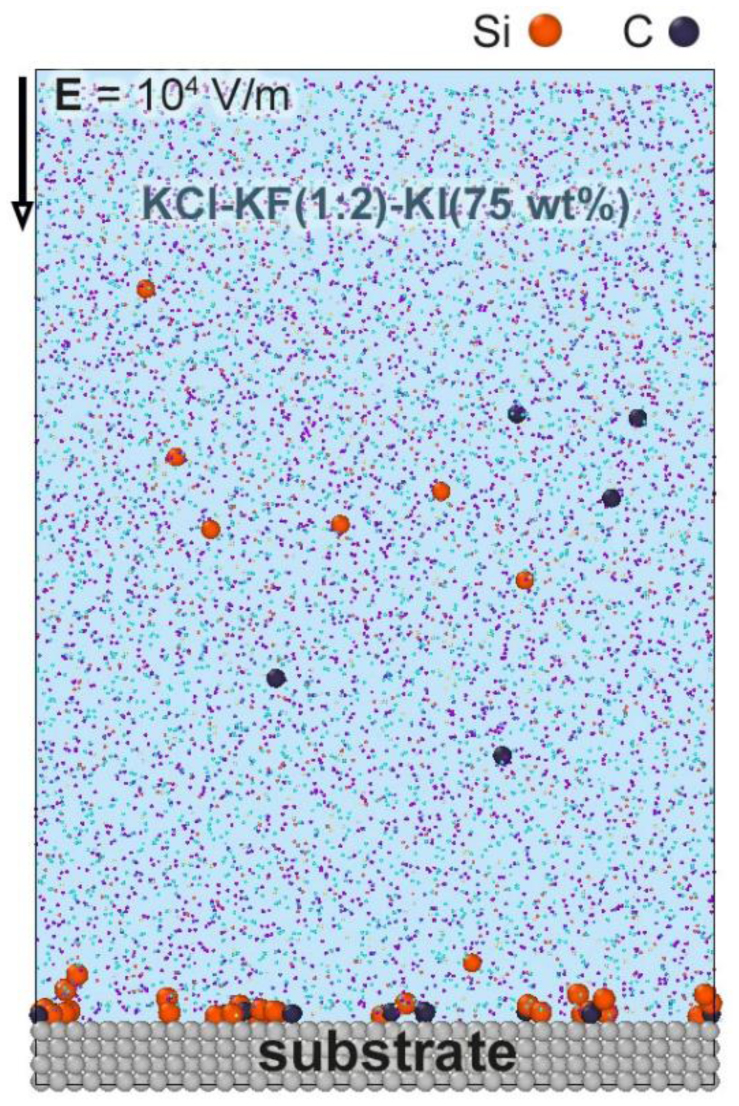
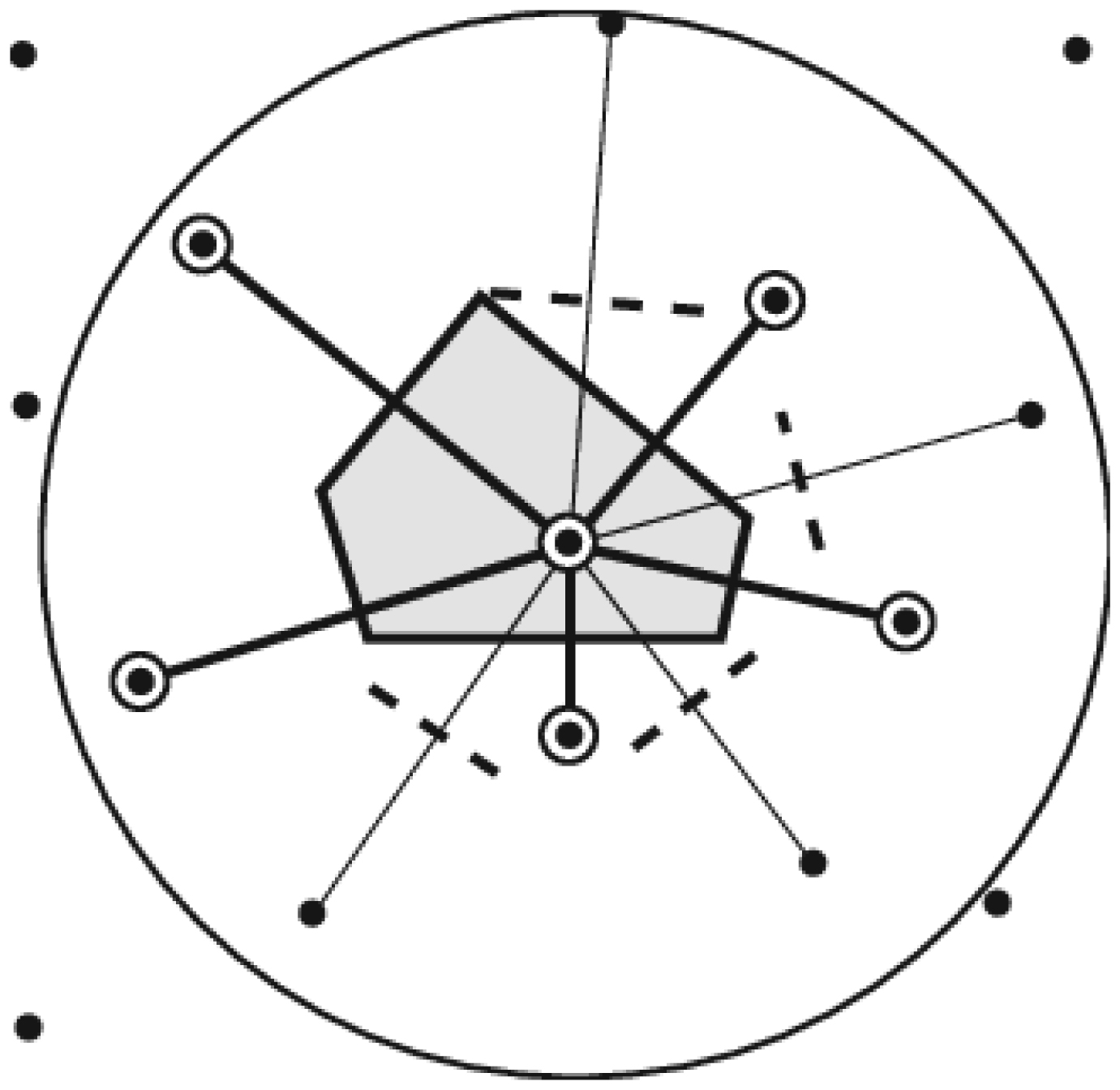
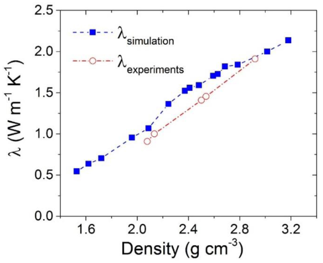
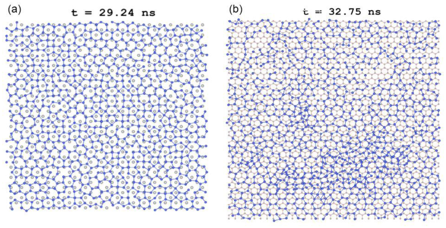
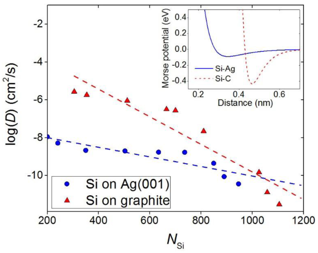
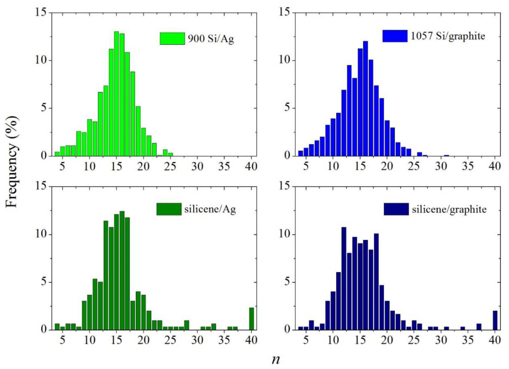
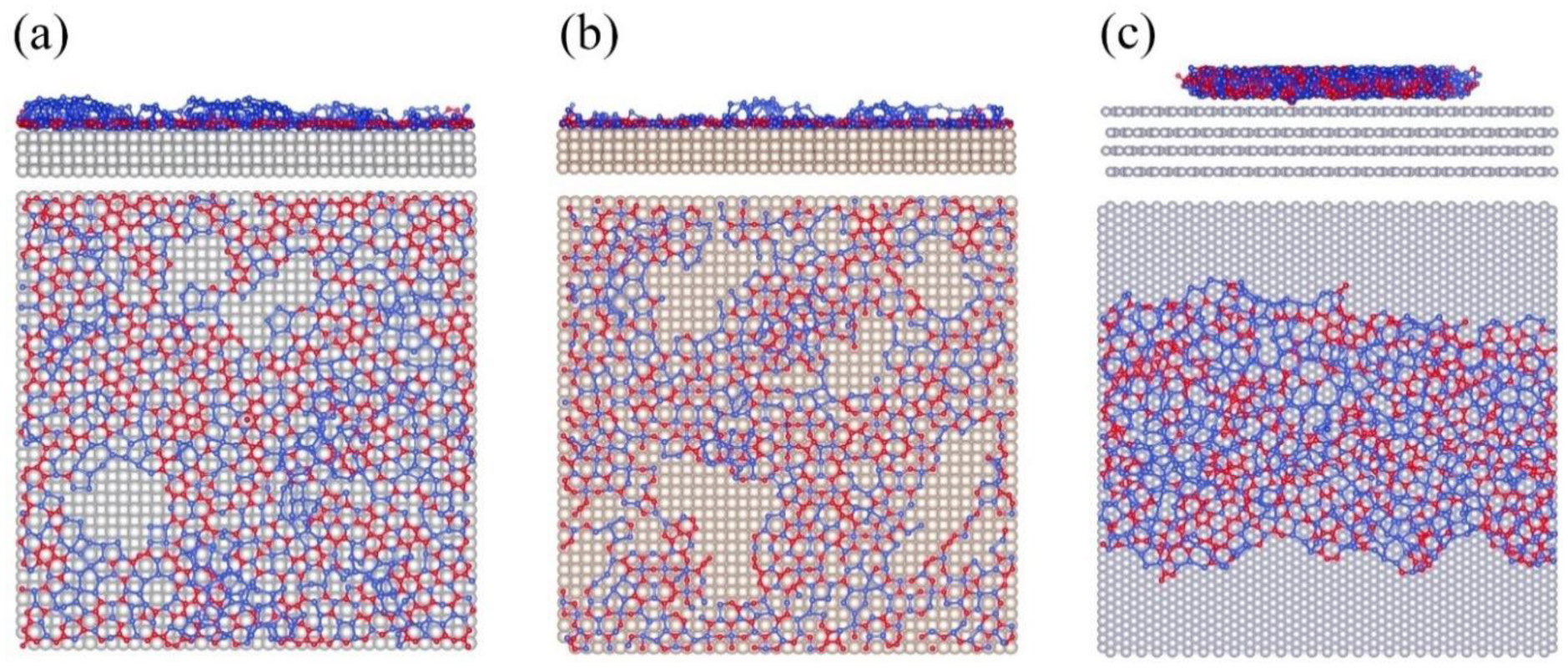
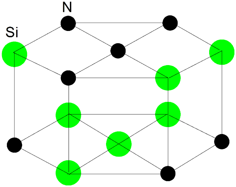
Optimizing the electrodeposition process condition requires considerable effort and time. The use of modeling and simulations can largely solve this problem. This short review is focused on the development of mathematical models and molecular dynamics simulations, which can be used to predict the electrodeposition of thin silicon and silicon carbide films using the KCl-KF-KI electrolyte. The use of computer simulations to obtain thin films of silicon nitride and silicon dioxide is considered. Silicon, silicon dioxide, silicon nitride, and silicon carbide are important biomedical materials. Additionally, we consider modeling the decomposition process of various precursors used as sources of Si4+ and C4+ ions for electrolytic deposition. The calculation of various physical properties of crystalline silicon and important modifications of silicon carbide, including the thermal conductivity, surface diffusion coefficients, and a detailed structure determined by constructing Voronoi polyhedra, are discussed. A computer model allows one to explore the use of “a defective silicene/silicon carbide” hybrid material as a lithium-ion battery anode. The possibilities for solving problems of processes optimization in modern methods for producing biomedical materials are discussed.
Citation: Alexander Galashev. Computer implementation of the method for electrolytic production of thin films for biomedical applications: short review[J]. AIMS Biophysics, 2024, 11(1): 39-65. doi: 10.3934/biophy.2024004
Optimizing the electrodeposition process condition requires considerable effort and time. The use of modeling and simulations can largely solve this problem. This short review is focused on the development of mathematical models and molecular dynamics simulations, which can be used to predict the electrodeposition of thin silicon and silicon carbide films using the KCl-KF-KI electrolyte. The use of computer simulations to obtain thin films of silicon nitride and silicon dioxide is considered. Silicon, silicon dioxide, silicon nitride, and silicon carbide are important biomedical materials. Additionally, we consider modeling the decomposition process of various precursors used as sources of Si4+ and C4+ ions for electrolytic deposition. The calculation of various physical properties of crystalline silicon and important modifications of silicon carbide, including the thermal conductivity, surface diffusion coefficients, and a detailed structure determined by constructing Voronoi polyhedra, are discussed. A computer model allows one to explore the use of “a defective silicene/silicon carbide” hybrid material as a lithium-ion battery anode. The possibilities for solving problems of processes optimization in modern methods for producing biomedical materials are discussed.

| [1] | Schoen FJ, Levy RJ, Tam H, et al. (2020) Pathological calcification of biomaterials. Biomaterials Science . London: Elsevier 973-994. https://doi.org/10.1016/B978-0-12-816137-1.00065-9 |
| [2] | Sastri VR (2013) Plastics in Medical Devices, Properties, Requirements, and Applications. Amsterdam: Elsevier. https://doi.org/10.1016/C2012-0-05946-7 |
| [3] |
Yesilirmak N, Altinors DD (2013) A silicone hydrogel contact lens after 7 years of continuous wear. Cont Lens Anterior Eye 36: 204-206. https://doi.org/10.1016/j.clae.2013.03.001 
|
| [4] | Saddow SE (2012) Silicon Carbide Biotechnology: A Biocompatible Semiconductor for Advanced Biomedical Devices and Applications. Amsterdam: Elsevier. https://doi.org/10.1016/C2014-0-03629-5 |
| [5] |
Oliveros A, Guiseppi-Elie A, Saddow SE (2013) Silicon carbide: a versatile material for biosensor applications. Biomed Microdevices 15: 353-368. https://doi.org/10.1007/s10544-013-9742-3
|
| [6] |
Cruz RLJ, Ross MT, Powell SK, et al. (2020) Advancements in soft-tissue prosthetics part B: The chemistry of imitating life. Front Bioeng Biotechnol 8: 147. https://doi.org/10.3389/fbioe.2020.00147
|
| [7] | Coletti C, Jaroszeski M, Pallaoro A, et al. (2007) Biocompatibility and wettability of crystalline SiC and Si surfaces. Proceedings of the 29th Annual International Conference of the IEEE Engineering in Medicine and Biology Society . Lyon, France: 5849-5852. https://doi.org/10.1109/IEMBS.2007.4353678 |
| [8] |
Saddow SE (2022) Silicon carbide technology for advanced human healthcare applications. Micromachines (Basel) 13: 346. https://doi.org/10.3390/mi13030346
|
| [9] |
Yunus G, Singh R, Raveendran S, et al. (2023) Electrochemical biosensors in healthcare services: bibliometric analysis and recent developments. PeerJ 11: e15566. https://doi.org/10.7717/peerj.15566
|
| [10] |
Jiang F, Liu Y, Yang Y, et al. (2012) Research progress of optical fabrication and surface-microstructure modification of SiC. J Nanomater 2012: 984048. https://doi.org/10.1155/2012/984048
|
| [11] | Marsil N, Majlis BY, Mohd-Yasin F, et al. (2020) A review: properties of silicon carbide materials in MEMS application. Int J Nanoelectron Mater 13: 113-128. http://hdl.handle.net/10072/411838 |
| [12] | Jani DB (2020) An overview on use of renewable solar energy in desiccant based thermal cooling systems. J Algerian Studies 1: 38-42. https://doi.org/10.5281/zenodo.4403022 |
| [13] |
Arvanitopoulos A, Antoniou M, Li F (2022) 3C-SiC-on-Si MOSFETs: Overcoming material technology limitations. IEEE T Ind Appl 58: 565-575. https://doi.org/10.1109/tia.2021.3119269
|
| [14] |
Toure M, Berenguier B, Kobor D (2018) Study by numerical simulation of a PN solar cell in 3C-SiC/Si. Afr J Environ Sci Technol 12: 532-537. https://doi.org/10.5897/AJEST2018.2565
|
| [15] |
Alkhaldi ND, Barman SK, Huda MN (2019) Crystal structures and the electronic properties of silicon-rich silicon carbide materials by first principle calculations. Heliyon 5: e02908. https://doi.org/10.1016/j.heliyon.2019.e02908
|
| [16] | Lynch ME, Mebane D, Liu M (2010) Numerical continuum modeling and simulation of mixed-conducting thin film and patterned electrodes. Ceramic Engineering and Science Proceedings 30: 129-138. https://doi.org/10.1002/9780470584316.ch12 |
| [17] |
Kang KH, Eun T, Jun MC, et al. (2014) Governing factors for the formation of 4H or 6H-SiC polytype during SiC crystal growth: An atomistic computational approach. J Cryst Growth 389: 120. https://doi.org/10.1016/j.jcrysgro.2013.12.007
|
| [18] | Fiorentis E, Gatou MA, Lagopati N, et al. (2023) Biomedical applications of silica (SiO2) nanoparticles. J Sci Tech Res 51: 42382-42389. https://doi.org/10.26717/BJSTR.2023.51.008057 |
| [19] |
Wei J, Ong PL, Tay FEH, et al. (2008) A new fabrication method of low stress PECVD SiNx layers for biomedical applications. Thin Solid Films 516: 5181-5188. https://doi.org/10.1016/j.tsf.2007.07.051
|
| [20] |
Andersson H, van den Berg A (2003) Microfluidic devices for cellomics: a review. Sens Actuators B: Chem 92: 315-325. https://doi.org/10.1016/S0925-4005(03)00266-1
|
| [21] |
Lin Z, Chen K, Zhang P, et al. (2017) Improved power efficiency in phosphorus doped n-a-SiNxOy/p-Si heterojunction light emitting diode. Appl Phys Lett 110: 081109. https://doi.org/10.1063/1.4977419
|
| [22] |
Paviet-Salomon B, Gall S, Monna R, et al. (2011) Laser doping using phosphorus-doped silicon nitrides. Energy Procedia 8: 700-705. https://doi.org/10. 1016/j.egypro.2011.06.204
|
| [23] |
Arl D, Roge V, Adjeroud N, et al. (2020) SiO2 thin film growth through a pure atomic layer deposition technique at room temperature. RSC Adv 10: 18073-18081. https://doi.org/10.1039/d0ra01602k
|
| [24] |
Gil-Ocaña V, Jimenez IM, Mayorga C, et al. (2021) Multiepitope dendrimeric antigen-silica particle composites as nano-based platforms for specific recognition of IgEs. Front Immunol 12: 750109. https://doi.org/10.3389/fimmu.2021.750109
|
| [25] |
Pandit B, Goda ES, Shaikh SF (2023) Electrochemical deposition toward thin films. Simple Chemical Methods for Thin Film Deposition: Synthesis and Applications . Singapore: Springer 245-304. https://doi.org/10.1007/978-981-99-0961-2-6
|
| [26] |
Yan Z, Liu R, Liu B, et al. (2023) Molecular dynamics simulation studies of properties, preparation, and performance of silicon carbide materials: a review. Energies 16: 1176. https://doi.org/10.3390/en16031176
|
| [27] |
Guan K, Zeng Q, Liu Y, et al. (2021) A multiscale model for CVD growth of silicon carbide. Comp Mater Sci 196: 110512. https://doi.org/10.1016/j.commatsci.2021.110512
|
| [28] | Bhowmik S, Raian AG (2022) Chemical vapor deposition of 2D materials: a review of modeling, simulation, and machine learning studies. Review 25: 103832. https://doi.org/10.1016/j.isci2022.103832 |
| [29] |
Wu K, Mei Q, Liu H, et al. (2023) Vapor deposition growth of SiC crystal on 4H-SiC substrate by molecular dynamics simulation. Crystals 13: 715. https://doi.org/10.3390/cryst13050715
|
| [30] |
Ivanichkina KA, Galashev AY, Isakov AV (2021) Computational modeling of electrolytic deposition of a single-layer silicon film on silver and graphite substrates. Appl Surf Sci 561: 149959. https://doi.org/10.1016/j.apsusc.2021.149959
|
| [31] |
Galashev AY, Abramova KA (2023) Computer simulation of obtaining thin films of silicon carbide. Phys Chem Chem Phys 25: 3834-3847. https://doi.org/10.1039/d2cp04208h
|
| [32] |
Laptev MV, Isakov AV, Grishenkova OV (2020) Electrodeposition of thin silicon films from the KF-KCl-KI-K2SiF6 melt. J Electrochem Soc 167: 04206. https://doi.org/10.1149/1945-7111/ab7aec
|
| [33] |
Ewald P (1921) Die Berechnung optischer und elektrostatischer Gitterpotentiale. Ann Phys-Berlin 369: 253-287. https://doi.org/10.1002/andp.19213690304
|
| [34] |
Hockney RW, Eastwood JW (1988) Computer Simulation Using Particles. Philadelphia: Taylor & Francis. https://doi.org/10.1201/9780367806934
|
| [35] |
Yu R, Zhai P, Li G, et al. (2012) Molecular dynamics simulation of the mechanical properties of single-crystal bulk Mg2Si. J Electron Mater 41: 1465-1469. https://doi.org/10.1007/s11664-012-1916-x
|
| [36] |
Foiles SM, Baskes MI, Daw MS (1986) Embedded-atom-methode functions for the fcc metals Cu, Ag, Au, Ni, Pd, Pt and their alloys. Phys Rev B 33: 7983. https://doi.org/10.1103/PhysRevB.33.7983
|
| [37] |
Tersoff J (1989) Modelng solid-state chemistry: Interatomic potentials for multicomponent systems. Phys Rev B: Condens Matter Mater Phys 39: 5566-5568. https://doi.org/10.1103/PhysRevB.39.5566
|
| [38] |
Daw MS, Baskes MI (1984) Embedded-atom method: Derivation and application to impurities, surfaces, and other defects in metals. Phys Rev B 29: 6443. https://doi.org/10.1103/PhysRevB.29.6443
|
| [39] |
Finney JL (1979) A procedure for the construction of Voronoi polyhedral. J Comput Phys 32: 137-143. https://doi.org/10.1016/0021-9991(79)90146-3
|
| [40] |
Galashev AE, Skripov VP (1984) Investigation on the disordering of the argon hexagonal closed packed (HCP) crystals by the method of statistical geometry. J Struct Chem 25: 734-740. https://doi.org/10.1007/BF00747917
|
| [41] |
Galashev AE, Ivanichkina KA (2017) Computational study of the properties of silicon thin films on graphite. Rus J Phys Chem A 91: 2448-2452. https://doi.org/10.1134/S003602441712007X
|
| [42] |
Filatova EA, Hausmann D, Elliott SD (2018) Understanding the mechanism of SiC plasma-enhanced chemical vapor deposition (PECVD) and developing routes toward SiC atomic layer deposition (ALD) with density functional theory. ACS Appl Mater Interfaces 10: 15216-15225. https://doi.org/10.1021/acsami.8b00794
|
| [43] |
Daoud S, Bouarissa N, Rekab-Djabri H, et al. (2022) Structural and thermo-physical properties of 3C-SiC: high-temperature and high-pressure effects. Silicon 14: 6299-6309. https://doi.org/10.1007/s12633-021-01387-8
|
| [44] |
Thakur S, Dionne CJ, Karna P, et al. (2022) Density and atomic coordination dictate vibrational characteristics and thermal conductivity of amorphous silicon carbide. Phys Rev Mater 6: 094601. https://doi.org/10.1103/PhysRevMaterials.6.094601
|
| [45] |
Isakov A, Apisarov A, Khudorozhkova AO, et al. (2018) Electrodeposition of silicon onto copper substrate from KF-KCl-KI-K2SiF6 melt. J Phys Conf Series 1134: 012021. https://doi.org/10.1088/1742-6596/1134/1/012021
|
| [46] |
Deng J, Liu JZ, Medhekar NV (2013) Enhanced lithium adsorption and diffusion on silicene nanoribbons. RSC Adv 3: 20338-20344. https://doi.org/10.1039/C3RA43326A
|
| [47] |
Galashev AY, Abramova KA (2023) Molecular dynamics simulation of thin silicon carbide films formation by the electrolytic method. Materials 16: 3115. https://doi.org/10.3390/ma16083115
|
| [48] |
Galashev AY, Rakhmanova OR (2022) Two-layer silicene on the SiC substrate: lithiation investigation in the molecular dynamics experiment. Chemphyschem 23: e202200250. https://doi.org/10.1002/cphc.20220
|
| [49] |
Galashev AE (2023) Computer simulation of a silicene anode on a silicon carbide substrate. Rus J Phys Chem B 17: 113-121. https://doi.org/10.1134/S1990793123010190
|
| [50] |
Galashev AE (2022) Computer test of a silicene/silicon carbide anode for a lithium ion battery. Rus J Phys Chem A 96: 2757-2762. https://doi.org/10.1134/S0036024422120123
|
| [51] |
Rajapakse M, Karki B, Abu UO, et al. (2021) Intercalation as a versatile tool for fabrication, property tuning, and phase transitions in 2D materials. NPJ 2D Mater Appl 5: 30. https://doi.org/10.1038/s41699-021-00211-6
|
| [52] | Bouhadiche A, Touam T (2018) Modeling and control of SiNx thin film surface morphology using kinetic Monte Carlo method. J Mater Sci 6: 134-140. https://doi.org/10.4172/2321-6212.1000224 |
| [53] |
Bouhadiche A, Difellah Z, Bouridah H, et al. (2023) Modeling and control of SiNx film growth using the kinetic Monte Carlo method: Impact of gas flow rate on surface roughness and film thickness. Silicon 15: 5209-5220. https://doi.org/10.1007/s12633-023-02415-5
|
| [54] |
Grigoriev FV, Sulimov VB, Tikhonravov AV (2022) Atomistic simulation of the ion-assisted deposition of silicon dioxide thin films. Nanomaterials 12: 3242. https://doi.org/10.3390/nano12183242
|
| [55] |
Takada A, Richet R, Catlow C (2004) Molecular dynamics simulations of vitreous silica structures. J Non-Cryst Solids 345–346: 224-229. https://doi.org/10.1016/j.jnoncrysol.2004.08.247
|
| [56] |
Abraham MJ, Murtola T, Schulz R, et al. (2015) GROMACS: high performance molecularsimulations through multi-level parallelism from laptops to supercomputers. SoftwareX 1–2: 19-25. https://doi.org/10.1016/j.softx.2015.06.001
|
| [57] |
Guo C, Kong M (2020) Fabrication of ultralow stress TiO2/SiO2 optical coatings by plasma ion-assisted deposition. Coatings 10: 720. https://doi.org/10.3390/coatings10080720
|
| [58] |
Dickinson EJF, Ekström H, Fontes E (2014) COMSOL Multiphysics®: Finite element software for electrochemical analysis. A mini-review. Electrochem Comm 40: 71-74. http://dx.doi.org/10.1016/j.elecom.2013.12.020
|
| [59] |
Datta A, Rakesh V (2009) An Introduction to Modeling of Transport Processes. Cambridge: Cambridge University Press. https://doi.org/10.1017/CBO9780511801150
|
| [60] |
Mandin P, Fabian C, Lincot D (2006) Importance of the density gradient effects in modelling electro deposition process at a rotating cylinder electrode. Electrochim Acta 51: 4067-4079. http://dx.doi.org/10.1016/j.electacta.2005.11.029
|
| [61] |
Hughes M, Strussevitch N, Bailey C, et al. (2010) Numerical algorithms for modelling electrodeposition: tracking the deposition front under forced convection from megasonic agitation. Int J Numer Methods Fluids 64: 237-268. http://dx.doi.org/10.1002/fld.2140
|
| [62] |
Mahapatro A, Suggu SK (2018) Modeling and simulation of electrodeposition: Effect of electrolyte current density and conductivity on electroplating thickness. Adv Mater Sci 3: 1-9. http://dx.doi.org/10.15761/AMS.1000143
|
| [63] |
Galashev AE, Ivanichkina KA (2019) Numerical simulation of the structure and mechanical properties of silicene layers on graphite during the lithium ion motion. Phys Solid State 61: 233-243. https://doi.org/10.1134/S1063783419020136
|
| [64] |
Wu D, Wang SW, Zhang SR, et al. (2019) Stabilization of two-dimensional penta-silicene for flexible lithium-ion battery via surface chemistry reconfiguration. Phys Chem Chem Phys 21: 1029-1037. https://doi.org/10.1039/c8cp05008b
|
| [65] |
Houssa M, Dimoulas A, Molle A (2015) Silicene: a review of recent of experimental and theoretical investigation. J Phys: Condens Matter 27: 253002. https://doi.org/10.1088/0953-8984/27/25/253002
|
| [66] |
Galashev AE, Ivanichkina KA, Vorobiyev AS, et al. (2017) Structure and stability of defective silicene on Ag(001) and Ag(111) substrates: a computer experiment. Phys Solid State 59: 1242-1252. https://doi.org/10.1134/S1063783417060087
|
| [67] |
Jamnig A, Pliatsikas N, Abadias G, et al. (1921) On the effect of copper as wetting agent during growth of thin silver films on silicon dioxide substrates. Appl Surf Sci 538: 148056. https://doi.org/10.1016/j.apsusc.2020.148056
|
| [68] |
Galashev AY, Vorob'ev AS (2020) Electronic and mechanical properties of silicene after nuclear transmutation doping with phosphorous. J Mater Sci 55: 11367-11381. https://doi.org/10.1007/s10853-020-04860-8
|
| [69] |
Zhang L, Cui Z (2022) First-principles study of metal impurities in silicon carbide: Structural, magnetic, and electronic properties. Front Mater 9: 956675. https://doi.org/10.3389/fmats.2022.956675
|
| [70] |
Kimoto T (2022) High-voltage SiC power devices for improved energy efficiency. Proc Jpn Acad Ser B Phys Biol Sci 98: 161-189. https://doi.org/10.2183/pjab.98.011
|
| [71] |
Ito Y, Nohira T (2000) Non-conventional electrolytes for electrochemical applications. Electrochim Acta 45: 2611-2622. https://doi.org/10.1016/S0013-4686(00)00341-8
|
| [72] |
Grillo F, Van Bui H, Moulijn JA, et al. (2017) Understanding and controlling the aggregative growth of platinum nanoparticles in atomic layer deposition: an avenue to size selection. J Phys Chem Lett 8: 975-983. https://doi.org/10.1021/acs.jpclett.6b02978
|
| [73] |
Mallik A, Ray BC (2011) Evolution of principle and practice of electrodeposited thin film: A review on effect of temperature and sonication. Int J Electrochem 2011: 8023. https://doi.org/10.4061/2011/568023
|
| [74] |
Zhang S, Fu H, Li T, et al. (2023) Study of effect of coil movement on growth conditions of SiC crystal. Materials (Basel) 16: 281. https://doi.org/10.3390/ma16010281
|
| [75] |
Zhang S, Fan G, Lic T, et al. (2022) Optimization of thermal field of 150 mm SiC crystal growth by PVT method. RSC Adv 12: 19936. https://doi.org/10.1039/d2ra02875a
|
| [76] |
Yang C, Liu G, Chen C, et al. (2018) Numerical simulation of temperature fields in a three-dimensional SiC crystal growth furnace with axisymmetric and spiral coils. Appl Sci 8: 705. https://doi.org/10.3390/app8050705
|
| [77] |
Ma RH, Zhang H, Ha S, et al. (2003) Integrated process modeling and experimental validation of silicon carbide sublimation growth. J Cryst Growth 252: 523-537. https://doi.org/10.1016/S0022-0248(03)00944-8
|
| [78] |
Manakov SM, Taurbavev NI (2012) Morphology and structural properties of a-Si:H and a-SiC:H films controlled in nanoscale. J Nanoelectron Optoelectron 7: 619-622. https://doi.org/10.1166/jno.2012.1402
|
| [79] |
Lebedev AA (1999) Deep level centers in silicon carbide: a review. Semiconductors 33: 107-130. https://doi.org/10.1134/1.1187657
|
| [80] | Wang M, Zhu F, Xu Y, et al. (2018) Investigation of the differences in nanometric grinding of SiC and Si by molecular dynamics. 2018 International Conference on Electronics Packaging and iMAPS, All Asia Conference (ICEP-IAAC) . Mie, Japan: IEEE. https://doi.org/10.23919/ICEP.2018.8374341 |
| [81] |
Samanta A, Grinberg I (2018) Investigation of Si/3C-SiC interface properties using classical molecular dynamics. J Appl Phys 124: 175110. https://doi.org/10.1063/1.5042203
|
| [82] |
Mazurek P, Vudayagiri S, Skov AL (2019) How to tailor flexible silicone elastomers with mechanical integrity: a tutorial review. Chem Soc Rev 48: 1448-1464. https://doi.org/10.1039/C8CS00963E
|
| [83] |
Li L, Li Y, Pei J, et al. (2023) Hotspots and trends of electrochemical biosensor technology: a bibliometric analysis from 2003 to 2023. RSC Adv 13: 30704-30717. https://doi.org/10.1039/D3RA05889A
|
Figures(17)

Alexander Galashev. Computer implementation of the method for electrolytic production of thin films for biomedical applications: short review[J]. AIMS Biophysics, 2024, 11(1): 39-65. doi: 10.3934/biophy.2024004


 DownLoad: