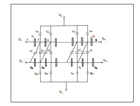
This work simulates and examines the circuit's operation for a single-electron nanostructure which is composed of slanted coupled two-dimensional arrays of tunnel junctions. The structure under study is modeled by combined computational simulation methods, both the Master Equation and the Monte-Carlo techniques. Throughout this process, the distribution of the time between successive random events could be computed at a reference junction. From these time distribution values, further calculations have been carried out to obtain the power spectral density trends, which reflect the corresponding properties on the frequency domain. For these homogeneous structures, the biasing conditions have been inspected for a combination of the two array's legs. It is found that, for some shorter lengths 3, 5, and up to 7 tunnel junctions could be triggered from any same or opposite side ends having different voltage polarities. For relatively longer structures of sizes 10, 15, 20, and 30 tunnel junctions, the circuit initial parameters are readjusted for obtaining remarkable results for their oscillations study. By increasing the value of the slanted coupling capacitance, the steady-state currents are in terms increased, and in this way, it is possible to realize the tunnel events correlations. It is shown that tuning the stray capacitances by slightly increasing their values will lead to a good clearer effect, especially for those longer array sets.
Citation: Nazim F. Habbani, Sharief F. Babikir. Study of single-electron tunneling oscillations using monte-carlo based modeling algorithms to a capacitive slanted two-dimensional array of tunnel junctions[J]. AIMS Electronics and Electrical Engineering, 2021, 5(1): 55-67. doi: 10.3934/electreng.2021004
This work simulates and examines the circuit's operation for a single-electron nanostructure which is composed of slanted coupled two-dimensional arrays of tunnel junctions. The structure under study is modeled by combined computational simulation methods, both the Master Equation and the Monte-Carlo techniques. Throughout this process, the distribution of the time between successive random events could be computed at a reference junction. From these time distribution values, further calculations have been carried out to obtain the power spectral density trends, which reflect the corresponding properties on the frequency domain. For these homogeneous structures, the biasing conditions have been inspected for a combination of the two array's legs. It is found that, for some shorter lengths 3, 5, and up to 7 tunnel junctions could be triggered from any same or opposite side ends having different voltage polarities. For relatively longer structures of sizes 10, 15, 20, and 30 tunnel junctions, the circuit initial parameters are readjusted for obtaining remarkable results for their oscillations study. By increasing the value of the slanted coupling capacitance, the steady-state currents are in terms increased, and in this way, it is possible to realize the tunnel events correlations. It is shown that tuning the stray capacitances by slightly increasing their values will lead to a good clearer effect, especially for those longer array sets.

| [1] |
Babiker S (2005) Simulation of single-electron transport in nanostructured quantum dots. IEEE T Electron Dev 52: 392-396. doi: 10.1109/TED.2005.843879

|
| [2] | Nielsen MA, Chuang IL (2000) Quantum computation and quantum information. Cambridge University Press, Cambridge, England. |
| [3] |
Matsuoka KA, Likharev KK (1998) Shot noise of single-electron tunneling in one-dimensional arrays. Phys Rev B 57: 15613-15622. doi: 10.1103/PhysRevB.57.15613
|
| [4] | Babiker SF, Bedri A (2012) Analysis of single-electron tunnelling oscillations in long arrays of tunnel junctions. IEEE SETIT, 6th International Conference: Sciences of Electronics, Technologies of Information and Telecommunications, 283-286. Tunisia. |
| [5] |
Hu GY, O'Connell RF, Ryu JY (1998) Slanted coupling of one-dimensional arrays of small tunnel junctions. J Appl Phys 84: 6713-6717. doi: 10.1063/1.368997
|
| [6] |
Habbani NF, Babikir SF (2020) Coherence of oscillations generated by single-electronic two-dimensional arrays of tunnel junctions. AIMS Electronics and Electrical Engineering 4: 188-199. doi: 10.3934/ElectrEng.2020.2.188
|
| [7] |
Likharev KK (1999) Single-electron devices and their applications. P IEEE 87: 606-632. doi: 10.1109/5.752518
|
| [8] |
Averin D, Likharev K (1986) Coulomb blockade of single-electron tunneling, and coherent oscillations in small tunnel junctions. J Low Temp Phys 62: 345–373. doi: 10.1007/BF00683469
|
| [9] | Hoekstra J (2009) Introduction to nanoelectronic single-electron circuit design. Pan Stanford Publishing Pte. Ltd. |
| [10] | Kouwenhoven LP, Markus CM, McEuen PL, et al. (1997) Electron transport in quantum dots. In: Mesoscopic Electron Transfer, 105-214. Dordrecht: Kluwer, Dordrecht. |
| [11] | Ingold GL, Nazarov YV (1992) Charge tunneling rates in ultra-small junctions, in Single Charge Tunneling. In: Single charge tunneling, 21-108. Springer. |
| [12] |
Averin DV, Likharev KK (1991) Single electronics: A correlated transfer of single electrons and cooper pairs in systems of small tunnel junctions. Modern Problems in Condensed Matter Sciences 30: 173-271 doi: 10.1016/B978-0-444-88454-1.50012-7
|
| [13] | Babiker S, Naeem R, Bedri A (2011) Algorithms for the static and dynamic simulation of single-electron tunnelling circuits. IET Circuits, Devices and Systems Journal. |
| [14] | Kirihara M, Kuwamura N, Taniguchi K, et al. (1994) Monte Carlo study of single- electronic devices. In: Ext. Abst. Int. Conf. Solid State Devices Mater., Yokohama, Japan, 328-330 |
| [15] |
Lindner B (2006) Superposition of many independent spike trains is generally not a Poisson process. Phys Rev E 73: 022901. doi: 10.1103/PhysRevE.73.022901
|
| [16] | Babiker S, Bedri AK (2011) Shot noise in long arrays of tunnel junctions. 2nd International Engineering Sciences Conference, Aleppo, Syria. |
| [17] | Babikir S, Alhassan ASA, Elhag NAA (2018) Coherence of oscillations generated by single electronic circuits. International Conference on Communication, Control, Computing and Electronics Engineering (ICCCCEE), Sudan. |


Figures(6) / Tables(3)

Nazim F. Habbani, Sharief F. Babikir. Study of single-electron tunneling oscillations using monte-carlo based modeling algorithms to a capacitive slanted two-dimensional array of tunnel junctions[J]. AIMS Electronics and Electrical Engineering, 2021, 5(1): 55-67. doi: 10.3934/electreng.2021004


 DownLoad: