Research article

Fabrication of aluminum microwires through artificial weak spots in a thick film using stress-induced migration

  • Received: 01 May 2018 Accepted: 27 June 2018 Published: 29 June 2018
  • With recent advances in technology, micro/nanomaterials have attracted a great deal of attention because of their superior properties compared with the bulk materials. Stress-induced migration (SM) has been used to fabricate micro/nanomaterials because of its advantages of simple processing, mass production, and the possibility of fabricating reactive materials such as aluminum. Stress-induced migration is a physical phenomenon of atomic diffusion driven by compressive stress gradients. When a multilayer structure that includes a passivation layer, a metallic film, and a substrate is heated, hydrostatic thermal stress gradients in the metallic film drive atoms to migrate and discharge through weak spots in the passivation layer. As a result, a large number of nanowhiskers and hillocks grow spontaneously at those locations. However, two problems exist in SM fabrication. First, the position, size, and shape of the growing materials are random because of the randomness of the weak spots. Second, fabricating microwires is difficult because migration of a large number of atoms is needed. In this study, 1-mm-diameter aluminum microwires were successfully grown at intended positions on thick aluminum film by using SM. The thick aluminum film was used to provide a sufficient number of atoms to form microwires. In addition, the positions of the microwires were controlled by introducing artificial weak spots. The parameters that are related to the intentional growth of microwires were investigated, and an optimum condition for growing aluminum microwires was presented.

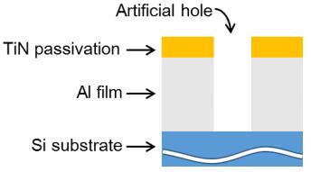
    Citation: Hsin-Tzu Lee, Yasuhiro Kimura, Masumi Saka. Fabrication of aluminum microwires through artificial weak spots in a thick film using stress-induced migration[J]. AIMS Materials Science, 2018, 5(4): 591-602. doi: 10.3934/matersci.2018.4.591

    Related Papers:

    [1] Dong Geun Lee, Hwan Chul Yoo, Eun-Ki Hong, Won-Ju Cho, Jong Tae Park . Device performances and instabilities of the engineered active layer with different film thickness and composition ratios in amorphous InGaZnO thin film transistors. AIMS Materials Science, 2020, 7(5): 596-607. doi: 10.3934/matersci.2020.5.596
    [2] Neerajkumar Wayzode, Vinod Suryawanshi . Mechanical properties of graphene nanoplatelets reinforced glass/epoxy composites manufactured using resin film infusion process. AIMS Materials Science, 2023, 10(4): 693-709. doi: 10.3934/matersci.2023038
    [3] Valeri S. Harutyunyan, Ashot P. Aivazyan, Andrey N. Avagyan . Stress field of a near-surface basal screw dislocation in elastically anisotropic hexagonal crystals. AIMS Materials Science, 2017, 4(6): 1202-1219. doi: 10.3934/matersci.2017.6.1202
    [4] Mohammed Tareque Chowdhury, Md. Abdullah Zubair, Hiroaki Takeda, Kazi Md. Amjad Hussain, Md. Fakhrul Islam . Optical and structural characterization of ZnSe thin film fabricated by thermal vapour deposition technique. AIMS Materials Science, 2017, 4(5): 1095-1121. doi: 10.3934/matersci.2017.5.1095
    [5] Stefan Wagner, Astrid Pundt . Hydrogen as a probe for defects in materials: Isotherms and related microstructures of palladium-hydrogen thin films. AIMS Materials Science, 2020, 7(4): 399-419. doi: 10.3934/matersci.2020.4.399
    [6] Ravipati Praveena, Gottapu. Varaprasada Rao, Karna Balasubrahmanyam, M. Ghanashyam Krishna, Vinjanampati Madhurima . Optical and water repellant properties of Ag/SnO2 bilayer thin films. AIMS Materials Science, 2016, 3(1): 231-244. doi: 10.3934/matersci.2016.1.231
    [7] Larysa Khomenkova, Mykola Baran, Jedrzej Jedrzejewski, Caroline Bonafos, Vincent Paillard, Yevgen Venger, Isaac Balberg, Nadiia Korsunska . Silicon nanocrystals embedded in oxide films grown by magnetron sputtering. AIMS Materials Science, 2016, 3(2): 538-561. doi: 10.3934/matersci.2016.2.538
    [8] Claas Hüter, Shuo Fu, Martin Finsterbusch, Egbert Figgemeier, Luke Wells, Robert Spatschek . Electrode–electrolyte interface stability in solid state electrolyte systems: influence of coating thickness under varying residual stresses. AIMS Materials Science, 2017, 4(4): 867-877. doi: 10.3934/matersci.2017.4.867
    [9] Wiebke Langgemach, Andreas Baumann, Manuela Ehrhardt, Thomas Preußner, Edda Rädlein . The strength of uncoated and coated ultra-thin flexible glass under cyclic load. AIMS Materials Science, 2024, 11(2): 343-368. doi: 10.3934/matersci.2024019
    [10] Sree Sourav Das, Zach Fox, Md Dalim Mia, Brian C Samuels, Rony Saha, Ravi Droopad . Demonstration of ferroelectricity in PLD grown HfO2-ZrO2 nanolaminates. AIMS Materials Science, 2023, 10(2): 342-355. doi: 10.3934/matersci.2023018
  • With recent advances in technology, micro/nanomaterials have attracted a great deal of attention because of their superior properties compared with the bulk materials. Stress-induced migration (SM) has been used to fabricate micro/nanomaterials because of its advantages of simple processing, mass production, and the possibility of fabricating reactive materials such as aluminum. Stress-induced migration is a physical phenomenon of atomic diffusion driven by compressive stress gradients. When a multilayer structure that includes a passivation layer, a metallic film, and a substrate is heated, hydrostatic thermal stress gradients in the metallic film drive atoms to migrate and discharge through weak spots in the passivation layer. As a result, a large number of nanowhiskers and hillocks grow spontaneously at those locations. However, two problems exist in SM fabrication. First, the position, size, and shape of the growing materials are random because of the randomness of the weak spots. Second, fabricating microwires is difficult because migration of a large number of atoms is needed. In this study, 1-mm-diameter aluminum microwires were successfully grown at intended positions on thick aluminum film by using SM. The thick aluminum film was used to provide a sufficient number of atoms to form microwires. In addition, the positions of the microwires were controlled by introducing artificial weak spots. The parameters that are related to the intentional growth of microwires were investigated, and an optimum condition for growing aluminum microwires was presented.


    1. Introduction

    Nowadays, micro/nanomaterials are indispensable for developing new technologies because of their good mechanical, electrical, and optical properties [1]. Various types of micro/nanomaterials have been fabricated and used in various applications [2,3,4]. For example, the Al micro/nanomaterials are used as plasmonic applications [5,6]. The fabrication of micro/nanomaterials can be roughly categorized as either a top-down or bottom-up approach. A top-down approach uses lithographic techniques to define patterns and etch away the unwanted parts. It can fabricate materials with good uniformity and is suitable for mass production. Nevertheless, this high-cost process has a resolution that is limited by the exposure wavelength. On the other hand, a bottom-up approach uses the self-assembly of atoms or molecules to form micro/nanomaterials. It can fabricate high-purity materials in small sizes. Bottom-up methods that use chemical solutions have been studied extensively. However, the processes that use these chemical methods require considerable skill, and the methods used to fabricate reactive materials such as aluminum are particularly difficult. On the other hand, methods using physical phenomenon can fabricate reactive materials with simple processes [7]. Among the physical methods, stress-induced migration (SM) is especially promising because of its advantages of simple processing and mass productivity.

    Stress-induced migration is a physical phenomenon of atomic diffusion driven by hydrostatic compressive stress gradients. This phenomenon occurs mostly in a multilayer structure, which is basically a system that includes a passivation layer (such as an oxide layer), a metallic film, and a substrate. When a hydrostatic compressive stress gradient exists in the metallic film, atoms are driven to migrate from higher compressive stress areas to lower compressive stress areas and discharge through weak spots in the passivation layer. Generally, in a metallic polycrystalline film, atoms migrate from grain boundaries to the insides of grains because stress concentrations happen at grain boundaries. Because of SM, a large number of nanowhiskers and hillocks have been observed growing spontaneously on multilayer devices. By intentionally using SM, whiskers and micro/nanomaterials can be fabricated [6,8].

    However, there are two problems with the fabrication of micro/nanomaterials through SM. First, there is the subject of controlling the fabrication. The spontaneously growing materials, especially nanomaterials, occur in random sizes and distributions because the weak spots are irregularly located. Furthermore, the shapes of the fabricated materials cannot be easily controlled. Another problem is the difficulty of fabricating microwires which need migration of a large number of atoms. Our team has studied the control of the positions of growing materials by introducing artificial holes in the passivation layer. Copper hillocks were grown at these artificial holes, and Cu whiskers were observed growing randomly on the tops of the hillocks [9]. By introducing holes, the positions of the copper hillocks were controlled; however, the fabrication of microwires at the hole locations was not achieved. Another study has examined the influence of various parameters related to the fabrication of silver whiskers [10]. It was reported that with an increasing thickness of the silver film, silver hillocks formed instead of whiskers. In another study [11], a change in shape from clearly-defined hillocks, such as triangular or rectangular, to round-shaped hillocks has been described according to the increasing thickness of the SiO2 passivation layer. Based on the above studies, it is expected that microwires can be fabricated at predetermined positions by introducing artificial holes and adjusting the thickness of each layer of a metallic film and a passivation layer.

    This study aimed to fabricate aluminum microwires at predetermined locations by using SM. To fabricate microwires, a sufficient number of atoms are required. Thick film was used because it can provide more atoms than thin film. Also, artificial holes were introduced as artificial weak spots in the passivation layer in order to control the locations of the microwires. In addition, a thick artificial passivation layer was used to prevent atoms from discharging freely. It should be noted that the aluminum film and passivation layer used in this study were much thicker than the structures treated in previous studies on the fabrication of aluminum materials, as shown in Table 1. By using this structure, 1-μm-diameter aluminum microwires were fabricated at the intended locations. Furthermore, experiments were done to investigate the influence of aluminum film thickness and passivation thickness on the fabrication.

    Table 1. Comparison of the thickness of the Al film and passivation layer in this study with previous studies.
    Chen et al. [12] Lu and Saka [13] Present study
    Al film 0.2 μm 0.15 μm ~3.60 μm
    Passivation layer Natural oxide Natural oxide or 2 nm SiO2 ~0.60 μm TiN
     | Show Table
    DownLoad: CSV

    2. Materials and method

    The structures of the samples are shown in Figure 1. A 3.60-μm-thick aluminum film was deposited on 280-μm-thick silicon (100) wafers at room temperature by radio frequency sputtering. Then, a 0.30-μm-thick TiN layer was deposited as passivation. TiN layer was used to prevent the diffusion of Al atoms into the passivation and the creation of intermetallic compound (IMC) between Al and the passivation, which impede to discharge Al atoms out from a hole. For investigating the influence of aluminum film thickness on the fabrication, two samples were made from 1.80- and 0.30-μm-thick aluminum film, respectively, under 0.30-μm-thick TiN passivation. Furthermore, to improve the result obtained by using the 1.80-μm-thick aluminum film, two samples were made with 0.45- and 0.60-μm-thick TiN passivation. After the deposition, focused ion beam (FIB) etching was used to create 1-μm-diameter holes that penetrated as far as the interface between the aluminum film and silicon substrate. The holes were made in 3 × 3 arrays on each sample. The distance between holes was wide enough (about 30 μm) that the migration around each hole would not be influenced by the others.

    Figure 1. Cross-sectional illustration of the samples.

    Before heating, the samples were observed using field emission scanning electron microscopy (FE-SEM), as shown in Figure 2. The samples were heated at a rate of 10 K/min to 773 K in an electric furnace, which was depressurized to −100 kPa, held for 3 h, and cooled in the furnace at a rate of 2 K/min. After heating, the samples were examined by FE-SEM and energy dispersive X-ray spectroscopy (EDX) elemental analysis. In addition, cross sections of the samples were made using FIB etching.

    Figure 2. FE-SEM micrograph of a sample before heating.

    3. Results and discussion


    3.1. Fabrication of aluminum microwires

    Figure 3 shows sample with 1-μm-diameter artificial holes in a structure of 0.30-μm-thick TiN passivation, 3.60-μm-thick aluminum film, and silicon substrate after heating. Aluminum microwires of 1-μm-diameter were grown at every hole although they were curled. One microwire was analyzed by EDX, as shown in Figure 4; and it was confirmed to be an aluminum microwire.

    Figure 3. FE-SEM micrograph of a sample using a structure of 0.30-μm-thick TiN passivation and 3.60-μm-thick aluminum film after heating.
    Figure 4. Results of EDX analyses of a microwire: (a) its FE-SEM micrograph, (b) its layered image; mapping images of (c) Al, (d) Ti, and (e) N.

    The mechanism of the intentional growth of microwires is explained as follows. Stress-induced migration is driven by a hydrostatic compressive stress gradient. The atomic flux of SM is given by [14,15]

    J=NΩDkBTgradσ (1)

    where N is the atomic density, Ω is the atomic volume, κB is Boltzmann's constant, T is the absolute temperature, and D is the diffusion coefficient. Furthermore, σ is the hydrostatic stress given by σ = (σx, f + σy, f + σz, f)/3, where σx, f, σy, f and σz, f are stresses within the film, in the Cartesian coordinate system shown in Figure 5. In this study, during heating, the stress gradient (gradσ) from inside of the thick film to the artificial hole surface caused atoms to migrate.

    Figure 5. Schematic illustration of the atomic migration around an artificial hole.

    It should be noted that gradσ cannot be created in the case of a thin film with thin passivation under the condition of plane stress. In traditional fabrication using SM, which considers a thin film on a substrate in the x–y plane and neglects the stress distribution in thickness direction, thermal stresses in the film can be expressed as [16]

    σx,f=σy,fEfΔT(αfαs)1νf (2)

    where E is Young's modulus, ν is Poisson's ratio, α is the thermal expansion coefficient, and ΔT is the temperature change. The subscript f denotes the thin film, and s denotes the substrate. Considering a case in which a thin film with a thin passivation layer on a substrate has a hole, even when the film is subjected to the above-mentioned stresses, gradσ from inside of the film to the hole surface does not exist because the hydrostatic thermal stress σ is uniform in the film. SM occurs from grain boundaries to grains [17], and micro/nanomaterials grow at the weak spots in the passivation layer rather than at the hole.

    On the other hand, as far as the thickness direction of a thin film with a thin passivation layer having no hole on a substrate is considered, gradσ can be nonzero in practice. Consider that inelastic strain ε0 is introduced into the thin film by some processes such as a mismatch in thermal expansion coefficients, which causes the stresses in the film and also causes the substrate to bend. The rigorous solution of Eq 2 is given by [18]

    σx,f=σy,f=κEs1νs(1+ρ3η)hs6ρ(1+ρ)+κEsη1νsz (3)

    where κ is the uniform bending curvature given by

    κ=6ρη(1+ρ)ε0hs(1+ρ4η2+4ρη+4ρη3+6ρ2η) (4)

    and ρ = hf/hs denoting the thickness by h, η = Ef(1 − νs)/(Es(1 − νf)), and z* is the distance along thickness direction above the midplane of the thin film. In the approximated situation where the film is much thinner than the substrate, Eq 3 reduces to Eq 2 by using ε0 = (αfαsT. Based on Eqs 3 and 4, gradσ in the thickness direction exists.

    From a different perspective, Settsu et al. [9] reported the creation of gradσ from inside of the film to the hole surface using a structure of artificial holes in a thin film with a thick passivation layer on a substrate. Because the thick passivation layer and substrate give uneven thermal stresses on top and bottom of the film, the stress distribution in the thickness direction cannot be neglected, and the thermal stresses in the x- and y-directions depend on the position in the thickness direction. Therefore, a hydrostatic gradσ is created from inside of the film to the hole surface. In this case, atoms accumulate at the holes instead of the grains. This is because the macroscopic hydrostatic stress gradient from inside of the film to the hole surface is much greater than the microscopic stress gradient from the grain boundaries to the grains. In addition, the migration from inside of the film to the hole surface is mainly by grain boundary diffusion, whereas the migration from the grain boundaries to the grains is by lattice diffusion, which is much slower.

    In this study, by using the structure of a thick film with a thick passivation layer on a substrate, gradσ was created in a manner similar to that in the study of Settsu et al. [9]. After the accumulating atoms filled up the hole, they created a stress gradient from the hole to the air, pushing atoms out. The holes played the role of artificial weak spots in the passivation layer, where stress relief happened by discharging atoms. Figure 5 shows a schematic illustration of the atomic migration around an artificial hole. The continuously accumulating atoms push other atoms upward, resulting in the growth of microwires from their bases [12].


    3.2. Effect of aluminum film thickness

    Next, the aluminum film thickness was decreased from 3.60 to 1.80 and 0.30 μm in order to see its influence on fabrication. In the sample that used 1.80-μm-thick aluminum film, large hillocks were formed instead of microwires, as shown in Figure 6a. In addition, the passivation layer around the holes was broken, as shown in the EDX analysis in Figure 7. In the sample that used 0.30-μm-thick aluminum film, almost nothing was formed, as shown in Figure 6b.

    Figure 6. FE-SEM micrographs of the samples using a structure of 0.30-μm-thick TiN passivation with (a) 1.80- and (b) 0.30-μm-thick aluminum film after heating.
    Figure 7. Results of EDX analyses of a large hillock: (a) its FE-SEM micrograph, (b) its layered image and mapping images of (c) Al, (d) Ti, (e) N, and (f) O.

    The formation process of the large hillocks is explained as follows. After migrating atoms accumulate and fill a hole, they are subjected to hydrostatic stress, which forces atoms to discharge from the hole. However, the wall of the hole in the passivation layer exerts a friction force, a so-called discharge resistance, to the atoms in a direction opposite to the discharging direction. This discharge resistance is considered to be proportional to the hydrostatic stress at the hole and is related to the materials, hole diameter, and passivation thickness. Because the atoms in the hole are subjected to the discharge resistance, they exert a reaction force to the discharge resistance back to the passivation layer. Eventually, the reaction force exceeds a critical value corresponding to the fracture strength of the passivation layer or the delamination strength of its interface with the aluminum film. When this happens, the passivation layer breaks by developing cracks in the passivation or by delamination at the interface. Once either one of the above fracture modes occurs, atoms in the hole move to a fracture site for stress relief, which contributes to the progress of the other fracture mode. When both the fracture and delamination of the passivation take place, atoms significantly discharge and form large hillocks. Therefore, the formation of large hillocks in the sample that used 1.80-μm-thick aluminum film indicated a larger reaction force to the discharge resistance (i.e., a larger hydrostatic stress in the holes). In this experiment, because the material and thickness of the passivation layers of the two samples were the same, formation of the large hillocks was attributed to the large hydrostatic stress at the holes.

    The reason for the higher stress in the sample using the 1.80-μm-thick aluminum film is believed to be the interaction between the aluminum film and silicon substrate, as shown by the cross-sectional morphologies in Figures 8 and 9. Whereas precipitation of silicon in aluminum was observed in the 1.80-μm-thick film (Figure 8), local diffusion of aluminum into silicon was observed in the 3.60-μm-thick film (Figure 9). The difference between these two samples is thought to have resulted from an increase in the solubility of silicon in aluminum with an increase in the film stress of aluminum [19]. In the 1.80-μm-thick film, where the residual film stress is lower, silicon atoms dissolved and then precipitated in the aluminum film, causing local compressive stress. This study infers that such local compressive stress resulted in large hydrostatic stress at the hole, which caused a large reaction force to the discharge resistance and broke the passivation layer. On the other hand, in the 3.60-μm-thick aluminum film, where the residual film stress was higher, the solubility is also higher, so more silicon atoms dissolved in this film than in the thinner film; more importantly, no silicon atoms precipitated in the aluminum film. Therefore, no local compressive stress was generated in the 3.60-μm-thick film, and hydrostatic stress at the hole was lower. In addition, many silicon atoms dissolved in the aluminum, leaving a large empty volume in the silicon substrate for the aluminum atoms to diffuse in. The above explanation matches a previous study, which reported that the precipitation of silicon in aluminum happens under low compressive stress, whereas the dissolution of silicon in aluminum happens under high compressive stress [20].

    Figure 8. A 30°-tilted cross-sectional view of the sample using 1.80-μm-thick aluminum film: (a) FE-SEM micrograph, (b) its EDX mapping analysis, and (c) the EDX line analysis from A to A' presented in (a).
    Figure 9. A 30°-tilted cross-sectional view of the sample using 3.60-μm-thick aluminum film: (a) a FE-SEM micrograph, and (b) its EDX mapping analysis.

    As for the sample that used 0.30-μm-thick aluminum film, the migration was considered too small to form microwires because the grain boundaries in thin film are less than those in thick film. Grain boundaries are the diffusion pathways of atoms, so fewer grain boundaries indicate less migration. Hence, it is difficult to use thin aluminum film in the fabrication of microwires.


    3.3. Effect of TiN passivation thickness

    Here, if the passivation layer in the sample that used 1.80-μm-thick aluminum film was not broken, microwires might have been fabricated instead of the large hillocks. To improve the result in the sample that used 1.80-μm-thick aluminum film, the passivation thickness was increased from 0.30 to 0.45 and 0.60 μm to suppress the breaking of the passivation layer because a thicker passivation layer has higher fracture and delamination strengths. The results are shown in Figure 10. The percentages of broken passivation layers (i.e., the percentages of large hillocks) under different passivation thicknesses are shown in Figure 11. Obviously, by increasing the passivation thickness, breaking of the passivation layer was eliminated, and microwires were fabricated. It should be noted that although some breaking of the passivation layer happened in the sample that used a 0.60-μm-thick passivation layer, its percentage was still much lower than that in the sample that used a 0.30-μm-thick passivation layer. As a result, an increase of the passivation thickness is still considered an effective way to eliminate the large hillocks and encourage the growth of microwires.

    Figure 10. FE-SEM micrographs of the samples using a structure of (a) 0.45- and (c) 0.60-μm-thick passivation with 1.80-μm-thick aluminum film after heating.
    Figure 11. The percentages of each shape of the fabricated materials under different passivation thicknesses. Each percentage is calculated as the number of each shape divided by the total number of the holes. If the aspect ratio of the fabricated material is less than 5, the material is categorized as a small hillock; if the ratio is larger, it is a microwire; and if breaking of the passivation occurs, the material is categorized as a large hillock.

    4. Conclusions

    In this study, 1-μm-diameter aluminum microwires were successfully fabricated at predetermined positions using SM although they were curled. The sample structure was 0.30-μm-thick TiN passivation, 3.60-μm-thick aluminum film, and silicon substrate with 1-μm-diameter holes. It was demonstrated that microwires could not be fabricated using a thin aluminum film. In addition, although the passivation layer was broken when the aluminum film thickness was decreased to 1.80 μm, such breakage was suppressed by increasing the passivation thickness (i.e., using the structure of 0.45- and 0.60-μm-thick TiN passivation, 1.8-μm-thick aluminum film, and silicon substrate). This study overcame the difficulties in the control of fabricating micromaterials with realizing migration of a large number of atoms.


    Acknowledgments

    This work was supported by JSPS KAKENHI Giant-in Aid for Scientific Research (B) No. 26289001.


    Conflict of interest

    The authors declare that there is no conflict of interest regarding the publication of this manuscript.


    [1] Sarkar J, Khan GG, Basumallick A (2007) Nanowires: Properties, applications and synthesis via porous anodic aluminium oxide template. B Mater Sci 30: 271–290. doi: 10.1007/s12034-007-0047-0
    [2] Tang JF, Tseng ZL, Chen LC, et al. (2016) ZnO nanowalls grown at low-temperature for electron collection in high-efficiency perovskite solar cells. Sol Energ Mat Sol C 154: 18–22. doi: 10.1016/j.solmat.2016.04.034
    [3] McKone JR, Warren EL, Bierman MJ, et al. (2011) Evaluation of Pt, Ni, and Ni–Mo electrocatalysts for hydrogen evolution on crystalline Si electrodes. Energ Environ Sci 4: 3573–3583. doi: 10.1039/c1ee01488a
    [4] Li C, Ji W, Chen J, et al. (2007) Metallic aluminum nanorods: Synthesis via vapor-deposition and applications in Al/air batteries. Chem Mater 19: 5812–5814. doi: 10.1021/cm7018795
    [5] Knight MW, King NS, Liu L, et al. (2014) Aluminum for plasmonics. ACS Nano 8: 834–840. doi: 10.1021/nn405495q
    [6] Ye F, Burns MJ, Naughton MJ (2015) Stress-induced growth of aluminum nanowires with a range of cross-sections. Phys Status Solidi A 212: 566–572. doi: 10.1002/pssa.201431618
    [7] Lu Y, Tohmyoh H, Saka M (2012) Comparison of stress migration and electromigration in the fabrication of thin Al wires. Thin Solid Films 520: 3448–3452. doi: 10.1016/j.tsf.2011.12.054
    [8] Cheng YT, Weiner AM, Wong CA, et al. (2002) Stress-induced growth of bismuth nanowires. Appl Phys Lett 81: 3248–3250. doi: 10.1063/1.1515885
    [9] Settsu N, Saka M, Yamaya F (2008) Fabrication of Cu nanowires at predetermined positions by utilising stress migration. Strain 44: 201–208. doi: 10.1111/j.1475-1305.2007.00370.x
    [10] Tohmyoh H, Yasuda M, Saka M (2010) Controlling Ag whisker growth using very thin metallic films. Scripta Mater 63: 289–292. doi: 10.1016/j.scriptamat.2010.04.013
    [11] Saka M, Yasuda M, Tohmyoh H, et al. (2008) Fabrication of Ag micromaterials by utilizing stress-induced migration. 2008 2nd Electronics System-Integration Technology Conference, Greenwich, UK, 507–510.
    [12] Chen M, Yue Y, Ju Y (2012) Growth of metal and metal oxide nanowires driven by the stress-induced migration. J Appl Phys 111: 104305. doi: 10.1063/1.4718436
    [13] Lu Y, Saka M (2013) Effect of surface film on the Al whisker fabrication by utilizing stress migration. Adv Mater Res 630: 110–113.
    [14] Herring C (1950) Diffusional viscosity of a polycrystalline solid. J Appl Phys 21: 437–445. doi: 10.1063/1.1699681
    [15] Korhonen MA, Børgesen P, Tu KN, et al. (1993) Stress evolution due to electromigration in confined metal lines. J Appl Phys 73: 3790–3799. doi: 10.1063/1.354073
    [16] Blachman AG (1971) Stress and resistivity control in sputtered molybdenum films and comparison with sputtered gold. Metall T 2: 699–709. doi: 10.1007/BF02662724
    [17] Saka M, Yamaya F, Tohmyoh H (2007) Rapid and mass growth of stress-induced nanowhiskers on the surfaces of evaporated polycrystalline Cu films. Scripta Mater 56: 1031–1034. doi: 10.1016/j.scriptamat.2007.02.036
    [18] Bower AF (2010) Applied Mechanics of Solids, Boca Raton: CRC Press, 697–698.
    [19] Mii H, Senoo M, Fujishiro I (1976) Solid solubility of Si in Al under high pressure. Jpn J Appl Phys 15: 777–783. doi: 10.1143/JJAP.15.777
    [20] Sankur H, McCaldin JO, Devaney J (1973) Solid-phase epitaxial growth of Si mesas from Al metallization. Appl Phys Lett 22: 64–66. doi: 10.1063/1.1654558
  • This article has been cited by:

    1. Yasuhiro Kimura, Yang Ju, Residual stress effect governing electromigration-based free-standing metallic micro/nanowire growth behavior, 2020, 116, 0003-6951, 024102, 10.1063/1.5131710
    2. Alex C. Campos, Suane C. Paes, Bruno S. Correa, Gabriel A. Cabrera-Pasca, Messias S. Costa, Cleidilane S. Costa, Larissa Otubo, A. W. Carbonari, Growth of Long ZnO Nanowires with High Density on the ZnO Surface for Gas Sensors, 2020, 3, 2574-0970, 175, 10.1021/acsanm.9b01888
    3. Yebo Lu, Quan Sun, Chuncheng Zuo, Chengli Tang, Haijun Song, Chao Li, Fabrication of Ag micro-particles based on stress-induced migration by using multilayered structure with artificial holes array, 2021, 104, 0036-8504, 003685042110381, 10.1177/00368504211038182
    4. Yasuhiro KIMURA, Electromigration-Driven Crystallinity Design of Metallic Nanowire, 2022, 71, 0514-5163, 735, 10.2472/jsms.71.735
    5. ThomasHeinrich Ludwig, Hironori Tohmyoh, Rapid growth of ultra-long Al whiskers from TiN/Al/Si island structures, 2021, 574, 00220248, 126311, 10.1016/j.jcrysgro.2021.126311
    6. Marina Romanova, Joris More-Chevalier, Michal Novotny, Petr Pokorny, Lenka Volfova, Premysl Fitl, Raimonds Poplausks, Yuri Dekhtyar, Thermal Stability of Black Aluminum Films and Growth of Aluminum Nanowires from Mechanical Defects on the Film Surface during Annealing, 2022, 259, 0370-1972, 2100467, 10.1002/pssb.202100467
    7. Yasuhiro Kimura, Yi Cui, Takamasa Suzuki, Yuki Tanaka, Takaaki Tanaka, Yuhki Toku, Yang Ju, Growth of metal nanowire forests controlled through stress fields induced by grain gradients, 2024, 385, 0036-8075, 641, 10.1126/science.adn9181
  • Reader Comments
  • © 2018 the Author(s), licensee AIMS Press. This is an open access article distributed under the terms of the Creative Commons Attribution License (http://creativecommons.org/licenses/by/4.0)
通讯作者: 陈斌, bchen63@163.com
  • 1. 

    沈阳化工大学材料科学与工程学院 沈阳 110142

  1. 本站搜索
  2. 百度学术搜索
  3. 万方数据库搜索
  4. CNKI搜索

Metrics

Article views(4554) PDF downloads(889) Cited by(7)

Article outline

Figures and Tables

Figures(11)  /  Tables(1)

Other Articles By Authors

/

DownLoad:  Full-Size Img  PowerPoint
Return
Return

Catalog