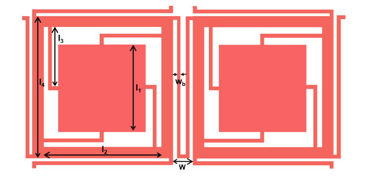
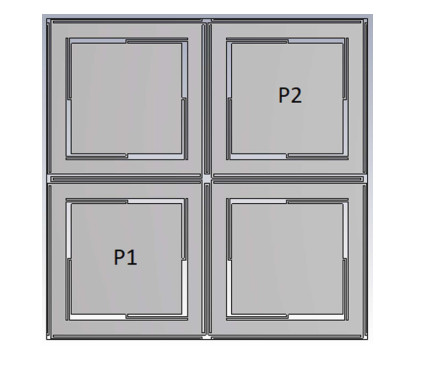
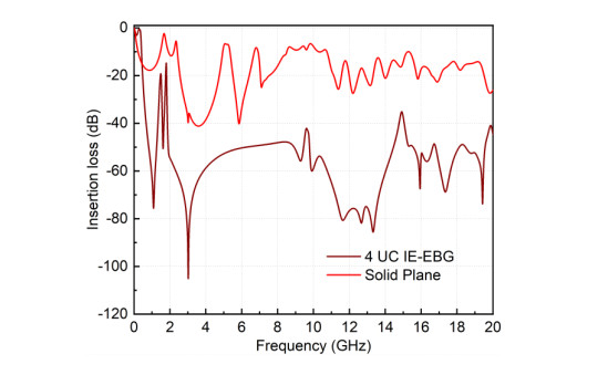
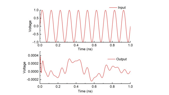
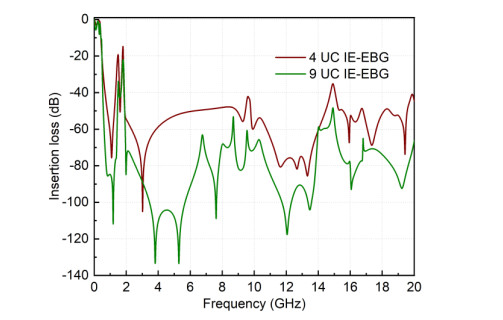
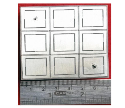
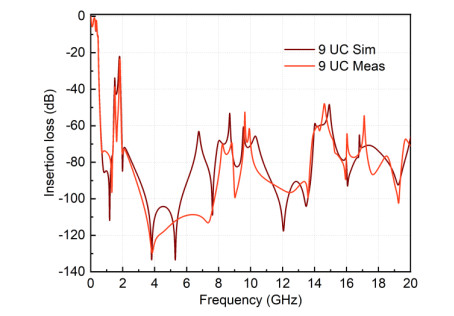
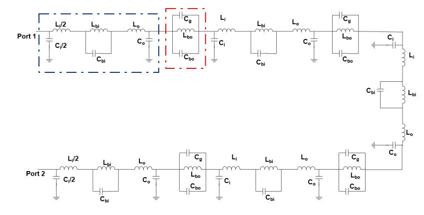
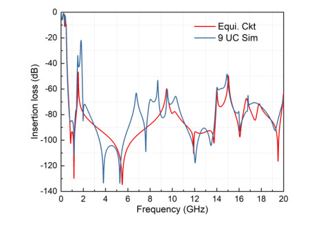
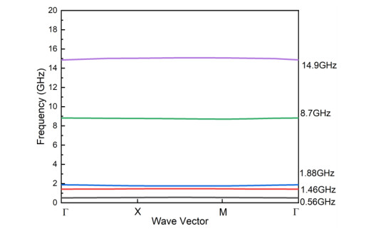
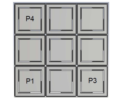
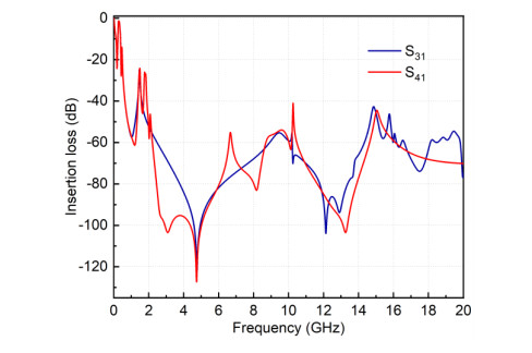
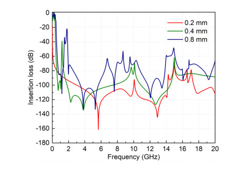
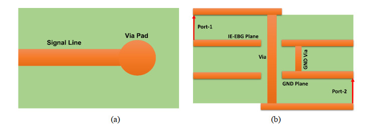
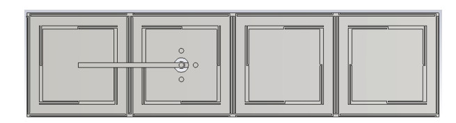
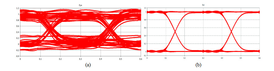
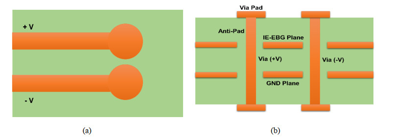
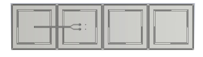
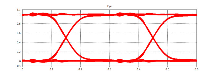
This paper proposes Inductive Enhanced-Electromagnetic Bandgap (IE-EBG) structure to suppress the Ground Bounce Noise (GBN) for high-speed digital system applications. The GBN excited between the power and ground plane pair could be a source of interference to the adjacent analog IC's on the same PCB (or) nearby devices because of radiated emission from the PCB edges. Hence, it must be suppressed at the PCB level. The proposed two-dimensional IE-EBG patterned power plane suppressed the GBN effectively over a broad frequency range. The four unit-cell IE-EBG provides a -40 dB noise suppression bandwidth of 13.567 GHz. With a substantial increment in the overall area, the nine unit-cell IE-EBG provides a -50 dB bandwidth of 19.02 GHz. The equivalent circuit modeling was developed for nine unit-cell IE-EBG and results are verified with the 3D EM simulation results. In addition, dispersion analysis was performed on the IE-EBG unit-cell to validate the lowest cut-off frequency and bandgap range. The prototype model of the proposed IE-EBG is fabricated and tested. The measured and simulated results are compared; a negligible variation is observed between them. In a multilayer PCB, the solid power plane is replaced with the 1 x 4 IE-EBG power plane and its impact on high-speed data transmission is analyzed with single-ended/differential signaling. The embedded IE-EBG with differential signaling provides optimum MEO and MEW values of 0.928 V, 0.293 ns for a random binary sequence with the 0.1 ns rise-time. Compared to single-ended signaling, embedded IE-EBG with differential signaling maintain good signal integrity and supports high-speed data transmission.
Citation: Vasudevan Karuppiah, UmaMaheswari Gurusamy. Compact EBG structure for ground bounce noise suppression in high-speed digital systems[J]. AIMS Electronics and Electrical Engineering, 2022, 6(2): 124-143. doi: 10.3934/electreng.2022008
This paper proposes Inductive Enhanced-Electromagnetic Bandgap (IE-EBG) structure to suppress the Ground Bounce Noise (GBN) for high-speed digital system applications. The GBN excited between the power and ground plane pair could be a source of interference to the adjacent analog IC's on the same PCB (or) nearby devices because of radiated emission from the PCB edges. Hence, it must be suppressed at the PCB level. The proposed two-dimensional IE-EBG patterned power plane suppressed the GBN effectively over a broad frequency range. The four unit-cell IE-EBG provides a -40 dB noise suppression bandwidth of 13.567 GHz. With a substantial increment in the overall area, the nine unit-cell IE-EBG provides a -50 dB bandwidth of 19.02 GHz. The equivalent circuit modeling was developed for nine unit-cell IE-EBG and results are verified with the 3D EM simulation results. In addition, dispersion analysis was performed on the IE-EBG unit-cell to validate the lowest cut-off frequency and bandgap range. The prototype model of the proposed IE-EBG is fabricated and tested. The measured and simulated results are compared; a negligible variation is observed between them. In a multilayer PCB, the solid power plane is replaced with the 1 x 4 IE-EBG power plane and its impact on high-speed data transmission is analyzed with single-ended/differential signaling. The embedded IE-EBG with differential signaling provides optimum MEO and MEW values of 0.928 V, 0.293 ns for a random binary sequence with the 0.1 ns rise-time. Compared to single-ended signaling, embedded IE-EBG with differential signaling maintain good signal integrity and supports high-speed data transmission.

| [1] |
Van den Berghe S, Olyslager F, De Zutter D, et al. (1998) Study of the ground bounce caused by power plane resonances. IEEE T Electromagn C 40: 111-119. https://doi.org/10.1109/15.673616 doi: 10.1109/15.673616

|
| [2] |
Lei GT, Techentin RW, Gilbert BK (1999) High-frequency characterization of power/ground-plane structures. IEEE T Microw Theory 47: 562-569. https://doi.org/10.1109/22.763156 doi: 10.1109/22.763156
|
| [3] |
Wu TL, Chen ST, Hwang JN, et al. (2004) Numerical and experimental investigation of radiation caused by the switching noise on the partitioned DC reference planes of high speed digital PCB. IEEE T Electromagn C 46: 33-45. https://doi.org/10.1109/TEMC.2004.823680 doi: 10.1109/TEMC.2004.823680
|
| [4] |
Muthana P, Srinivasan K, Engin AE, et al. (2008) Improvements in noise suppression for I/O circuits using embedded planar capacitors. IEEE T Adv Packaging 31: 234-245. https://doi.org/10.1109/TADVP.2008.920651 doi: 10.1109/TADVP.2008.920651
|
| [5] |
Wang TK, Han TW, Wu TL (2008) A novel power/ground layer using artificial substrate EBG for simultaneously switching noise suppression. IEEE T Microw Theory 56: 1164-1171. https://doi.org/10.1109/TMTT.2008.921642 doi: 10.1109/TMTT.2008.921642
|
| [6] |
Jaglan N, Kanaujia BK, Gupta SD, et al. (2018) Design of band-notched antenna with DG-CEBG. Int J Electron 105: 58-72. https://doi.org/10.1080/00207217.2017.1340977 doi: 10.1080/00207217.2017.1340977
|
| [7] |
Jaglan N, Gupta SD, Thakur E, et al. (2018) Triple band notched mushroom and uniplanar EBG structures based UWB MIMO/Diversity antenna with enhanced wide band isolation. AEU-Int J Electron C 90: 36-44. https://doi.org/10.1016/j.aeue.2018.04.009 doi: 10.1016/j.aeue.2018.04.009
|
| [8] |
Abdulhameed MK, Isa MM, Zakaria Z, et al. (2019). Novel design of triple-band EBG. Telkomnika 17: 1683-1691. https://doi.org/10.12928/telkomnika.v17i4.12616 doi: 10.12928/telkomnika.v17i4.12616
|
| [9] |
Abdulhameed MK, Isa MSB, Zakaria Z, et al. (2020) Enhanced performance of compact 2×2 antenna array with electromagnetic band‐gap. Microw Opt Techn Let 62: 875-886. https://doi.org/10.1002/mop.32092 doi: 10.1002/mop.32092
|
| [10] |
Al-Gburi AJAA, Ibrahim IMM, Zakaria Z, et al. (2021) Enhancing Gain for UWB Antennas Using FSS: A Systematic Review. Mathematics 9: 3301. https://doi.org/10.3390/math9243301 doi: 10.3390/math9243301
|
| [11] |
Wu TL, Lin YH, Wang TK, et al. (2005) Electromagnetic bandgap power/ground planes for wideband suppression of ground bounce noise and radiated emission in high-speed circuits. IEEE T Microw Theory 53: 2935-2942. https://doi.org/10.1109/TMTT.2005.854248 doi: 10.1109/TMTT.2005.854248
|
| [12] |
Wang TK, Hsieh CY, Chuang HH, et al. (2009) Design and modeling of a stopband-enhanced EBG structure using ground surface perturbation lattice for power/ground noise suppression. IEEE T Microw Theory 57: 2047-2054. https://doi.org/10.1109/TMTT.2009.2025466 doi: 10.1109/TMTT.2009.2025466
|
| [13] |
Hsieh CY, Wang CD, Lin KY, et al. (2010) A power bus with multiple via ground surface perturbation lattices for broadband noise isolation: Modeling and application in RF-SiP. IEEE T Adv Packaging 33: 582-591. https://doi.org/10.1109/TADVP.2009.2036858 doi: 10.1109/TADVP.2009.2036858
|
| [14] |
Kim M, Kam DG (2015) Wideband and compact EBG structure with balanced slots. IEEE T Comp Pack Man 5: 818-827. https://doi.org/10.1109/TCPMT.2015.2436404 doi: 10.1109/TCPMT.2015.2436404
|
| [15] |
Shi LF, Li KJ, Hu HQ, et al. (2015) Novel L-EBG embedded structure for the suppression of SSN. IEEE T Electromagn C 58: 241-248. https://doi.org/10.1109/TEMC.2015.2505736 doi: 10.1109/TEMC.2015.2505736
|
| [16] |
Appasani B, Verma VK, Pelluri R, et al. (2017) Genetic algorithm optimized electromagnetic band gap structure for wide band noise suppression. Prog Electrom Res Le 71: 109-115. https://doi.org/10.2528/PIERL17091204 doi: 10.2528/PIERL17091204
|
| [17] |
Kim Y, Cho J, Cho K, et al. (2017) Glass-interposer electromagnetic bandgap structure with defected ground plane for broadband suppression of power/ground noise coupling. IEEE T Comp Pack Man 7: 1493-1505. https://doi.org/10.1109/TCPMT.2017.2730853 doi: 10.1109/TCPMT.2017.2730853
|
| [18] |
Ning C, Jin J, Yang K, et al. (2017) A novel electromagnetic bandgap power plane etched with multiring CSRRs for suppressing simultaneous switching noise. IEEE T Electromagn C 60: 733-737. https://doi.org/10.1109/TEMC.2017.2731783 doi: 10.1109/TEMC.2017.2731783
|
| [19] |
Shi LF, Sun ZM, Liu GX, et al. (2017) Hybrid-embedded EBG structure for ultrawideband suppression of SSN. IEEE T Electromagn C 60: 747-753. https://doi.org/10.1109/TEMC.2017.2743039 doi: 10.1109/TEMC.2017.2743039
|
| [20] |
Engin AE, Ndip I, Lang KD, et al. (2017) Nonoverlapping power/ground planes for suppression of power plane noise. IEEE T Comp Pack Man 8: 50-56. https://doi.org/10.1109/TCPMT.2017.2764801 doi: 10.1109/TCPMT.2017.2764801
|
| [21] |
Hsieh HC, Chan HW, Wang YC, et al. (2019) Nonperiodic Flipped EBG for Dual-Band SSN Mitigation in Two-Layer PCB. IEEE T Comp Pack Man 9: 1690-1697. https://doi.org/10.1109/TCPMT.2019.2933490 doi: 10.1109/TCPMT.2019.2933490
|
| [22] |
Zhu HR, Sun YF, Huang ZX, et al. (2018) A compact EBG structure with etching spiral slots for ultrawideband simultaneous switching noise mitigation in mixed signal systems. IEEE T Comp Pack Man 9: 1559-1567. https://doi.org/10.1109/TCPMT.2018.2888512 doi: 10.1109/TCPMT.2018.2888512
|
| [23] |
Zhang F, Ding PP, Yang GM, et al. (2020) A Novel Double-Square Electromagnetic Bandgap Structure for Wideband SSN Suppression in High-Speed PCB. IEEE T Electromagn C 62: 2585-2594. https://doi.org/10.1109/TEMC.2020.2982014 doi: 10.1109/TEMC.2020.2982014
|
| [24] |
Mohajer-Iravani B, Ramahi OM (2009) Wideband circuit model for planar EBG structures. IEEE T Adv Packaging 33: 169-179. https://doi.org/10.1109/TADVP.2009.2021156 doi: 10.1109/TADVP.2009.2021156
|
Figures(21) / Tables(8)

Vasudevan Karuppiah, UmaMaheswari Gurusamy. Compact EBG structure for ground bounce noise suppression in high-speed digital systems[J]. AIMS Electronics and Electrical Engineering, 2022, 6(2): 124-143. doi: 10.3934/electreng.2022008


 DownLoad: