Research article

Design and simulation of a CMOS image sensor with a built-in edge detection for tactile vision sensory substitution

  • Received: 10 January 2019 Accepted: 27 March 2019 Published: 06 May 2019
  • Tactile Vision Sensory Substitution (TVSS) systems are used to convert scene images captured by the image sensors to tactile patterns that can be used to stimulate the skin sensory of the blind users. These types of devices needed to be wearable, small size, low power consumption, lightweight, and affordable cost. This paper presents the integration of an edge detection scheme inside a CMOS image sensor forming an Edge Detection CMOS Image Sensor (EDIS). The design is simulated using LTSPICE and MATLAB, performing three ways of simulation, giving accepted edge images having very few fine edges but keeping the main edges. The proposed way is simple, low component-count, doesn’t reduce the fill factor, use no analog to digital converter, presents adaptable comparator-reference-voltage, and make a step towards an integrated all-in-one tactile vision sensory substitution device.

    Citation: Mazin H. Aziz , Saad D. Al-Shamaa. Design and simulation of a CMOS image sensor with a built-in edge detection for tactile vision sensory substitution[J]. AIMS Electronics and Electrical Engineering, 2019, 3(2): 144-163. doi: 10.3934/ElectrEng.2019.2.144

    Related Papers:

    [1] Deven Nahata, Kareem Othman . Exploring the challenges and opportunities of image processing and sensor fusion in autonomous vehicles: A comprehensive review. AIMS Electronics and Electrical Engineering, 2023, 7(4): 271-321. doi: 10.3934/electreng.2023016
    [2] M V Raghunathareddy, G Indumathi, K R Niranjan . Highly sensitive optical MEMS based photonic biosensor for colon tissue detection. AIMS Electronics and Electrical Engineering, 2022, 6(3): 285-295. doi: 10.3934/electreng.2022017
    [3] Farhan Khan, Sing Kiong Nguang . Dual sensing scheduling algorithm for WSN based road network surveillance. AIMS Electronics and Electrical Engineering, 2021, 5(1): 38-54. doi: 10.3934/electreng.2021003
    [4] Benaoumeur Ibari, Mourad Hebali, Baghdadi Rezali, Menaouer Bennaoum . Collision detection and external force estimation for robot manipulators using a composite momentum observer. AIMS Electronics and Electrical Engineering, 2024, 8(2): 247-264. doi: 10.3934/electreng.2024011
    [5] Shahzad Ashraf, Arshad Ahmad, Adnan Yahya, Tauqeer Ahmed . Underwater routing protocols: Analysis of link selection challenges. AIMS Electronics and Electrical Engineering, 2020, 4(3): 234-248. doi: 10.3934/ElectrEng.2020.3.234
    [6] Abdelkrim Abanay, Lhoussaine Masmoudi, Mohamed El Ansari, Javier Gonzalez-Jimenez, Francisco-Angel Moreno . LIDAR-based autonomous navigation method for an agricultural mobile robot in strawberry greenhouse: AgriEco Robot. AIMS Electronics and Electrical Engineering, 2022, 6(3): 317-328. doi: 10.3934/electreng.2022019
    [7] Sundararajan Seenivasaan, Naduvil Madhusoodanan Kottarthil . Enhancing sensor linearity through the translinear circuit implementation of piecewise and neural network models. AIMS Electronics and Electrical Engineering, 2023, 7(3): 196-216. doi: 10.3934/electreng.2023012
    [8] Vasileios Delimaras, Kyriakos Tsiakmakis, Argyrios T. Hatzopoulos . Analog interface based on capacitance multiplier for capacitive sensors and application to evaluate the quality of oils. AIMS Electronics and Electrical Engineering, 2023, 7(4): 243-270. doi: 10.3934/electreng.2023015
    [9] Minglong Zhang, Iek Cheong Lam, Arun Kumar, Kin Kee Chow, Peter Han Joo Chong . Optical environmental sensing in wireless smart meter network. AIMS Electronics and Electrical Engineering, 2018, 2(3): 103-116. doi: 10.3934/ElectrEng.2018.3.103
    [10] Mostafa A.R. Eltokhy, Mohamed Abdel-Hady, Ayman Haggag, Hisham A. Hamad, Tarek Hosny, Ahmed A. F. Youssef, Ali M. El-Rifaie . An indoor IoT-based LiFi system using LEDs for sensor data transfer. AIMS Electronics and Electrical Engineering, 2025, 9(2): 118-138. doi: 10.3934/electreng.2025007
  • Tactile Vision Sensory Substitution (TVSS) systems are used to convert scene images captured by the image sensors to tactile patterns that can be used to stimulate the skin sensory of the blind users. These types of devices needed to be wearable, small size, low power consumption, lightweight, and affordable cost. This paper presents the integration of an edge detection scheme inside a CMOS image sensor forming an Edge Detection CMOS Image Sensor (EDIS). The design is simulated using LTSPICE and MATLAB, performing three ways of simulation, giving accepted edge images having very few fine edges but keeping the main edges. The proposed way is simple, low component-count, doesn’t reduce the fill factor, use no analog to digital converter, presents adaptable comparator-reference-voltage, and make a step towards an integrated all-in-one tactile vision sensory substitution device.


    Any TVSS system consists mainly of an image sensor, an image processing unit and a tactile display. The tactile display involves an array of tactile stimulators which transfer the scene visual image to the user's skin with minimum details to avoid sensory overload while respecting the spatial resolution of the skin's sensory receptors [1,2,3,4]. The main job of the image processing unit is to generate a tactile pattern, for the scene image, without losing its important features. One of the main used ways to do that is by converting the captured image to an edge, boundary or contour image [5,6,7,8,9]. This was enhanced by research results showing that the human retina is related to extraction of edge information from an incident image [10,11]. The desired features of the edge images for TVSS system are essentially accomplished by applying one of the first order edge detection algorithms in order to enhance the main edges and exclude the detail edges [12,13,14,15,16,17,18,19]. Anyway, some research has applied a different approach to finding edges of the scene image [20].

    To take a step towards the production of an all-in-one TVSS device, this paper presents the design and simulation of an EDIS. EDIS is mostly tailored for a certain demand. The benefits of using EDIS are reviewed here in addition to the review of some literature. History of microelectronics tells that integration leads to greater reliability, lower system power, and plummeting system cost/performance ratios. CMOS-based imaging systems on a chip can be expected to reflect these long-standing trends as they will be developed over the next years [21]. Low-level image processing on the sensor focal plane produces a smart sensor device called a retina which makes vision systems more compact, offering fast and parallel processing, but needs optimal design architecture for every vision algorithm [22], with improved image quality in comparison with the standalone digital processing, [23] offering lower manufacturing cost [24]. Research in the field of image sensor design, simulation, and implementation continues to produce a smart image sensor that mimics the biological retina where the pixel-level processing promises high SNR [25]. Markus Loose et al. [26] have implemented a CMOS Image Sensor (CIS) having (20 × 20) pixels of adaptive photoreceptors, modeled on a biological example, to be used for tactile vision. The design of a CMOS active pixel sensor (APS) chip has been described by R.H. Nixon et al. with integrated digital control functions forming a camera-on-a-chip having a 256 × 256 APS sensor [27]. System-level architectures and design methodology was presented [28]. An event detection CIS based on relative change in intensity was produced [29]. CIS readout strategy performing edge detection, to overcome the excessive output data flow bottleneck, was emulated by MATLAB, with circuit simulations using the Cadence Spectra Simulator [30]. The Bioinspired CIS may add visual tracking, detection, recognition, simultaneous localization and mapping, reconstruction, stereo matching, and control [31].

    Roberts has presented one of the earliest first order edge detection methods, the cross operator [32,33]. Roberts' method "fails to detect fine edges" [34], which is considered an asset thing in the generation of the tactile patterns. Operator's convolution with the image is widely used for edge detection using software or DSP tools while Applying convolution in analog processing earns little interest and consumes more hardware elements. This paper presents the implementation and simulation of Roberts' method inside the CMOS image sensor to get an edge image that can be converted to a tactile pattern.

    CIS simulation has been applied using SPICE models for Si and GaAs pin photodetectors [35]. An optoelectronic simulation that included time, power, and wavelength-domain behaviors was presented [36]. On the other hand, and to overcome the long time needed for simulation, a graphical toolbox was developed in Cadence Analog Design Environment (ADE). It permitted to manipulate images as input and automatically generate images at output [37], which is improved later [38,39]. Another approach was also introduced by M. R. Jha et al [40]. CIS with 8T global shutter and the 3T APS was simulated using Virtuoso analog design environment [41]. Other works have presented a combination of the circuit level and functional level simulation [42,43].

    The typical parts of the CIS (Figure 1) are the photodetector (PD), charge to voltage converter, source follower (SF), and analog to digital converter (ADC). The CIS basic block diagram is sketched in Figure 2, it consists of an array of pixels, vertical access part, horizontal access part, and the readout part. The PD array is a two-dimensional matrix of pixels that resemble the function of the retina. A readout circuit is a one-dimensional array of switches, sample & hold (S/H) circuits, and some storage elements. Access units are used to reach a certain pixel by enabling a certain row and a certain column.

    Figure 1.  Typical parts of a CIS.
    Figure 2.  The basic block diagram of the image sensor.

    The photodetector is integrated with other components to form the sensor cell or the photo pixel. Many types of pixels were introduced over the last three decades. They are classified mainly as passive pixel sensors (PPSs), active pixel sensors (APSs), and digital pixel sensors (DPSs). While PPS directly transfers the accumulated signal charges to the outside of the pixel, APS converts the accumulated signal charges to a potential in the attached transistor [44]. APS was first produced by E. Fossum et al. at Jet Propulsion Laboratory (JPL) using a photogate (PG), and then using a photodiode (PD), as a photodetector [45,46]. PS can also be classified according to the number of transistors per pixel, like three transistors APS (3T-APS), 4T-APS, 5T-APS [47], 2.5T-APS, and so on. Decimal fraction of transistors' number per pixels is due to transistor sharing with adjacent pixels which depends on the design and readout mechanism. As the number of transistors per pixel increases, the fill factor (FF) decreases.

    The photodetector is mostly a p-n junction photodiode, but phototransistor, pinned PD (PPD), photogate (PG), or Gate/Body-Tied Photodetector (GBT [48,49,50] can be used. PPD CIS represent today the main solid-state optical sensor technology for imaging applications ranging from mass-market smartphones to high-end scientific instruments [51]. It is used in most of CCD and CIS due to its low noise, high quantum efficiency, and low dark current [52,53]. The PPD is almost used in the 4T-APS.

    This paper presents the design and simulation of an Edge Detection Image Sensor (EDIS), which is an IS with a built-in edge detector. It was based on Roberts' algorithm and was applied to the binary image. The proposed way was verified and compared with some other ways of edge detection using MATLAB. Then designed and simulated using the compact SPICE models. The simulation was implemented using a circuit level model and a small size CIS model via LTSPICE. A third simulation was done using both MATLAB and LTSPICE to perform a fast simulation with image-in image-out for any resolution of the input image.

    The proposed technique was based on applying XOR function between every two vertices of the diagonals of 2 × 2 subarray, then obtaining the OR result of them (Figure 3). It was applied using a sliding window, having a height of two rows of pixels, slides from top to the bottom of the photo pixels array as shown in Figure 4.

    Figure 3.  The implemented edge detection way using XOR for (a) the right-down diagonal vertices, (b) left-down diagonal vertices (c) and taking the OR result of the combination of both.
    Figure 4.  The implemented edge detection that was based on the siding window technique having two-row height, slides from top to the bottom on the PD array.

    The following steps were applied, using MATLAB, to check the validity of the proposed way:

    1. read the input image and if it is an RGB image convert it to the gray level,

    2. convert the gray to binary using a threshold level,

    3. detect the change of state between the (i, j)th pixel and the (i+1, j+1)th pixel by XOR function using the formula (1),

    4. detect the change of state between the (i, j)th pixel and the (i-1, j+1)th pixel using XOR function using the formula (2),

    5. combine the two outputs using OR function (3),

    6. repeat the above three steps to the end of the current row, and

    Ixor1(i,j)=I(i,j)XORI(i+1,j+1)where:i=1:N1and   j=1:M1 (1)
    Ixor2(i,j)=I(i,j)XORI(i+1,j+1)where:i=2:N1andj=1:M1 (2)
    IEdge(i,j)=(Ixor1)OR(Ixor2) (3)

    7. slide down one row and repeat the above 4 steps while moving down until the last row.

    The flow of an image through this verification steps is shown in Figure 5.

    Figure 5.  A flow of an image through the proposed verification steps using MATLAB. The drawing of black on white was used for clarity.

    Some parts of the image sensor that are used in this design are explained here. These units are the photo pixel circuit, the column control circuit, the comparator, the XOR circuit, the NOR circuit, and the readout unit. The design efforts were mainly focused on the array of the photo pixels and the readout circuitry to fulfill the edge detection demand.

    The 4T-APS pixel with Pinned PD (PPD) was selected to be used in the proposed design. The accumulated photocharge in the junction capacitor CPD (Figure 6) is passed to the floating diffusion capacitor CFD via the transfer gate M2. M1 transistor, when activated by the RST signal, pushes up the FD node to (VDD - Vth(M1)) voltage level. While when M1 is OFF, the voltage on the FD node is transferred to M4 via the NMOS Source Follower (NMOS SF) transistor M4. M3 is the output stage of the pixel that transfers the pixel signal to M3 and is activated via the ROW control line. This process is repeated to all the rows of the image sensor array. The timing diagram of the photo pixel control signals is sketched in Figure 7. The time interval from two TX pulses is called the integration time because it is the time for photocurrent to accumulate or integrate the charge inside the PPD.

    Figure 6.  Control signals timing.
    Figure 7.  The 4T-APS circuit cascaded to the CCNT circuit and the column line capacitance CLC. (1) Column line current source. (2) S/H with S/H capacitance. (3) S/H control signal generator used for simulation. (4) PMOS SF buffer. (5) The output buffer current source.

    The column control circuit (CCNT) contains the sample and hold (S/H) circuit, column line biasing transistor, and output buffering as shown in Figure 6. The output of the CCNT unit is fed to a comparator unit along with a reference voltage (VR) in order to convert the analog signal level to a binary level.

    The simplified block diagram of the proposed IS is illustrated in Figure 8 without the edge detection circuit. An entire row of pixels is selected using the signal ROWi, hence, the voltage of each pixel in that row (only) is passed to its corresponding column line, cached into the (S/H) capacitor, passed to the comparator circuit, and compared with a reference voltage (VR) controlled by the user. The output is a binary signal that represents the photo-detected signals of the pixels at the ith row for all the CIS columns, stored temporarily in M-number D latches (for an N × M PD array). At each frame, only one row is selected, and its data is stored at the D-FF latches using the CLK signal as shown in Figure 9. In this design, there is no need for the Analog to Digital Conversion (ADC). The stored values form a line of the scene image in binary. To apply the proposed edge detection technique, a second line of D-FFs was added to store the data of the neighbored row. Therefore at a given row time the first set stores the previous row, while the second stores the current row. The outputs of these two D-FFs are fed to the XOR-OR circuits to generate the points of the edge image and the results are stored in a third set of D-FFs (Figure 10). The whole operation is finished in a single-row interval. The XOR circuit used in this design is composed of three transistors [54]. A CMOS inverter and a PMOS pass transistor were used to act as a two inputs XOR gate. A complementary NOR gate design was selected due to its low power, high noise margins, and ease of design.

    Figure 8.  CIS simplified timing diagram.
    Figure 9.  A simplified block diagram of the CIS. The ith row is selected via control signal ROWi.
    Figure 10.  The PPD model circuit diagram; (a) Accurate, and (b) Simplified.

    We have applied three ways of simulation: the first; was the simulation of the individual circuits via LTSPICE electronic circuit simulation environment, the second was also via LTSPICE to simulate a CIS having a PD array of 8 × 8 pixels. While the third was a fast way through a combination of both MATLAB and LTSPICE.

    The simplified (pinned) photodiode model circuit diagram shown in Figure 11 was used in the simulation. The shunt resistor (RSH) and the series resistor (RS) were neglected, as in the most of the image sensor functional simulations, i.e. the shunt resistor is considered to be very high and the series resistor is very low. One of the advantages of the pinned photodiode is the very low dark current (IDark), therefore it was not included in the simulation model. The IPD current source was used to model the photocurrent. CPD is the parasitic capacitance of the P-N junction. It was found that CPD value changes with the voltage change at the photodiode cathode during the photocurrent integration period, and typically it is a few tens of fFs [55]. The control signals were generated using simulated voltage sources. Figure 12 shows the signal diagram, and Figure 13 demonstrates the simulated signals for five different photocurrent (IPD) values showing the signal voltages decrease with the increase of IPD input for the PD, FD and Sout nodes that were depicted in Figure 6.

    Figure 11.  On top: the block diagram of the 3-levels of D-ffs used to store the signals of the current row, the previous row and the resultant row. On bottom: their control signal timing. Rising edge is used to latch the input.
    Figure 12.  PD, FD and sout node voltages, for five different values of the IPD current, which reflects the illuminance levels.
    Figure 13.  The simulated input /output signals of the photopixel for IPD = 1000 pA, showing effects of the control signals on PD, FD and output nodes.

    The output of the photo pixel circuit (Sout) is passed to the input of the column control circuit (CCNT), and the simulation signals are sketched in Figure 14, in synchronization with the ROW signal. The comparator, XOR, NOR, and the remnant circuits were all simulated too.

    Figure 14.  CCNT signals in synchronization with the row-select signal.

    An overall functional simulation was performed using a PD array of 8 × 8 pixels. Signals of the important nodes of the CIS circuits were monitored for various inputs and conditions. Each pixel of the PD array was equipped with its own IPD variable current source, to simulate the reflected light from a certain point of the scene. This current source is, essentially, a part of the PD simulation model, and was drawn off to the outside of the pixel to simplify the simulation procedure, thus a certain input pattern representing a scene image could be given to the CIS. We have found empirically that IPD value range that sustains linear characteristics of the designed APS was from 0.0 nA to 1.66 nA. Figure 15 illustrates the circuit diagram used in this simulation. Many input patterns were used in the simulation, one of them was a diagonal line consisting of the pixels P (3, 6), P (4, 5), P (5, 4) and P (6, 3). Where all the pixels of the PD array were fed with an IPD = 1.0 nA and the diagonal line pixels with an IPD = 0.5 nA. An extra control signal, the frame start (Fstr), was added to synchronize the periphery unit with the first pixel of the current image frame. The timing diagram for this case is sketched in Figure 16. It is not easy to judge the result through this form, therefore, a new look of the diagram is presented in Figure 17, by rotating right the previous timing diagram by 90̊, and paste a small black rectangle to each zero-level of the output waveform. The results had proved the functionality of the proposed EDIS.

    Figure 15.  The simulation cct. for the 8 × 8 CIS. The input is an IPD for each PD. The output is a single row, from the edge image, at a time. The timing and control signal generators are not included in the figure.
    Figure 16.  The timing and control signals sketched with EDIS output waveforms for about 2-frame. The shaded area is a frame of 8 × 7 pixels sketched in the time domain.
    Figure 17.  (Left) The test input image pattern. (Right) The output (90º rotated timing diagram) with black rectangles being pasted on the zero levels.

    Fast simulation is used to overcome the limitations of CIS simulation with its full PD array size. It is based on the reduction of the number of calculations from the variable number of pixels, forming the array, to a fixed number depends on the gray levels (256) for the input image and on the resolution of the ADC (if used) [37,38,39,43]. The output of the CIS is an edge image, where every pixel relates to an input-pixel, or pixels, by a certain relationship or function. This relationship was extracted from the previous LTSPICE simulation of the proposed design. The simulation was repeated for 256 times by sweeping the input IPD from 0.0 nA to 1.66 nA in a step of 6.484 pA (1.66nA/256). For each step of the input, the output of the column control circuit was recorded in lock-up-table 1 (LUT1) and the comparator output was recorded in LUT2. These two LUTs were used as a real substitution of the CIS-SPICE macro models and inserted in a MATLAB simulation program that was written for that purpose (Figure 18). The input image was converted to gray levels, then each gray level was mapped to an IPD level (0–1.6 nA), then converted (via LUT1 or LUT2) to a voltage level, at last, the XOR-OR function is applied to find the resultant edge image can select either hardware or software comparison.

    Figure 18.  The block diagram of the fast simulation.

    The simulation of the 8 × 8 pixels EDIS has given edge's pattern for any input image as depicted in Figure 17 for example. Parametric results were listed in Table 1, in comparison with previous works.

    Table 1.  Comparison of the proposed EDIS results with four research results.
    References M. Nam [56] C. Soell [57]* C. Lee [58] James A [59] The Proposed*
    Power Supply (V) 1.8 1.8 1.6 --- 3.3
    # of Transistors per pixel 3T + 9T (bump) ---- 2T + 12T (VCRO) --- 4T
    Simulation --- MATLAB, Cadence with 3×3 pixels readout Monte Carlo CUDA LTSPICE, MATLAB, Fast of both
    ADC Type --- 1-bit None None None
    Pixel Array 64×64 200×200 105×92 Variable Variable
    Frame Rate (F/s) 1302@ 10µs 504@ 30 µs 75 30 --- 195
    Edge Detection Technique Bump cct. Sobel Digital RTLN** Sliding Row NOR-XOR
    Pixel Complexity High --- High --- Minimum
    Power per pixel (nW) 900 -- 27.7 --- 0.708
    Power (mW) -- 5.5 8 --- ---
    * Simulated, ** Resistive Threshold Logic Network with CMOS flash memories.

     | Show Table
    DownLoad: CSV

    Results of the fast simulation can be demonstrated in many forms. The first was performed to check the validity of the proposed way when subjected to downscaling which is essential for TVSS applications. Figure 19 shows 5 images with different original resolutions passed to the fast simulation process for two times to get the 256 × 256 and 64 × 64 output pixels edge images respectively.

    Figure 19.  Examples showing inputs and outputs for 5 images. (Top) input images having different resolutions. (Middle) output edge's images using a resolution of 256 × 256 pixels. (Bottom) output edge's images but the resolution is 64 × 64 pixels.

    Another test was done to check the device response to the reference voltage (VR) variation. User's controlled VR, can give the blind person the required tactile image detail's level. An example is shown in Figure 20.

    Figure 20.  An example demonstrating the effects of altering VR.

    Results of visual comparisons with the results of some of the previous works are presented in Figures 2124.

    Figure 21.  Comparision with, M.Nam and K.Cho results [57].
    Figure 22.  Comparison with the result of simulation by C. Soell et al [58].
    Figure 23.  Comparison with a result of the simulation by C. Lee et al [59].
    Figure 24.  Comparison with a result of James A et al. [60].

    The proposed way had given acceptable edge images, and it was validated by the simulation using LTSPICE and MATLAB. Parametric comparison with some previous works have shown acceptable results, as well as the visual comparison of the edge images.

    This paper has presented the design and simulation of an Edge Detection CMOS Image Sensor (EDIS) to satisfy the demands of TVSS systems. An edge detection technique based on Roberts's has been converted to a simple hardware scheme conserving APS-fill factor as well as eliminating the use of ADC. The design functionality has been verified using a fast simulation technique. The design of this IS can be considered a step towards the production of an all-in-one TVSS device. The design can be improved by adding a Correlated Double Sampling (CDS) circuit to improve SNR in the future.

    The authors declare that there is no conflict of interest in this paper.


    [1] Kristjánsson Á, Moldoveanu A, Jóhannesson ÓI, et al. (2016) Designing sensory-substitution devices: Principles, pitfalls and potential1. Restor Neurol Neuros 34: 769–787.
    [2] Bach-y-Rita P, Kercel SW (2003) Sensory substitution and the human–machine interface.Trends Cogn Sci 7: 541–546. doi: 10.1016/j.tics.2003.10.013
    [3] Way TP, Barner KE (1997) Automatic Visual to Tactile Translation, Part I: Human Factors, Access Methods, and Image Manipulation. IEEE TRANSACTIONS ON REHABILITATION ENGINEERING 5: 81–94. doi: 10.1109/86.559353
    [4] Velázquez R (2010) Wearable assistive devices for the blind. In: Wearable and autonomous biomedical devices and systems for smart environment, pp. 331–349, Springer.
    [5] Krufka SE, Barner KE, Aysal TC (2007) Visual to tactile conversion of vector graphics. IEEE Transactions on Neural Systems and Rehabilitation Engineering 15: 310–321. doi: 10.1109/TNSRE.2007.897029
    [6] Ivanchenko V, Coughlan JM, Shen H (2008) Detecting and locating crosswalks using a camera phone. In: 2008 IEEE Computer Society Conference on Computer Vision and Pattern Recognition Workshops, pp. 1–8.
    [7] Bourbakis N (2008) Sensing surrounding 3-D space for navigation of the blind. IEEE Engineering in Medicine and Biology Magazine 27: 49–55. doi: 10.1109/MEMB.2007.901780
    [8] Balakrishnan G, Sainarayanan G, Nagarajan R, et al. (2007) Wearable Real-Time Stereo Vision for the Visually Impaired. Engineering Letters 14: 6–14.
    [9] Kajimoto H, Kanno Y, Tachi S (2006) Forehead Electro-tactile Display for Vision Substitution. In: Proc EuroHaptics.
    [10] Kong JS, Kim SH, Sung DK, et al. (2016) A 160×20 Light-Adaptive CMOS Vision Chip for Edge Detection Based on a Retinal Structure Using a Saturating Resistive Network. ETRI Journal 29: 59–69.
    [11] Katic N, Schmid A, Leblebici Y (2014) A retina-inspired robust on-focal-plane multi-band edge-detection scheme for CMOS image sensors. In: 2014 IEEE 57th International Midwest Symposium on Circuits and Systems (MWSCAS), pp. 683–686.
    [12] Jose J, Farrajota M, Rodrigues JMF, et al. (2011) The SmartVision local navigation aid for blind and visually impaired persons. International Journal of Digital Content Technology and its Applications 5: 362–375.
    [13] Kajimoto H, Suzuki M, Kanno Y (2014) HamsaTouch: Tactile vision substitution with smartphone and electro-tactile display. In: Proceedings of the Extended Abstracts of the 32nd annual ACM conference on Human Factors in Computing Systems, pp. 1273–1278.
    [14] Pereira MC, Kassab F (2006) An electrical stimulator for sensory substitution. In: 2006 International Conference of the IEEE Engineering in Medicine and Biology Society, pp. 6016–6020.
    [15] Rao AS, Gubbi J, Palaniswami M, et al. (2016) A vision-based system to detect potholes and uneven surfaces for assisting blind people. In: 2016 IEEE International Conference on Communications (ICC), pp. 1–6.
    [16] Roth P, Richoz D, Petrucci LS, et al. (2001) An audio-haptic tool for non-visual image representation. In: Proceedings of the 6th International Symposium on Signal Processing and Its Applications 1: 64–67.
    [17] Way TP, Barner KE (1997) Automatic Visual to Tactile Translation, Part II: Evaluation of the TACTile Image Creation System. International Conference of the IEEE Engineering in Medicine and Biology Society 5: 95–105.
    [18] du Buf JMH, Barroso J, Rodrigues JMF, et al. (2011) The SmartVision Navigation Prototype for Blind Users. International Journal of Digital Content Technology and its Applications 5: 351–361.
    [19] Hir JL, Kolar A, Santos FVD (2017) Distributed mixed-signal architecture for programmable smart image sensors. In: 2017 15th IEEE International New Circuits and Systems Conference (NEWCAS), pp. 353–356.
    [20] Grewe L, Overell W (2017) Road following for blindBike: an assistive bike navigation system for low vision persons. In: Signal Processing, Sensor/Information Fusion, and Target Recognition XXVI 10200: 1020011. doi: 10.1117/12.2264548
    [21] Fossum ER (1998) Digital camera system on a chip. IEEE Micro 18: 8–15.
    [22] Elouardi A, Bouaziz S, Dupret A, et al. (2007) Time comparison in image processing: APS sensors versus an artificial retina based vision system. Meas Sci Technol 18: 2817–2826. doi: 10.1088/0957-0233/18/9/011
    [23] Gonda M, Jarvis R (2000) Tactile Vision-Development of a Wearable Prosthesis for the Blind. In: Australian Conference on Robotics and Automation, pp. 71–74.
    [24] Elouardi A, Bouaziz S, Dupret A, et al. (2004) Image processing vision system implementing a smart sensor. In: Proceedings of the 21st IEEE Instrumentation and Measurement Technology Conference (IEEE Cat. No.04CH37510) 1: 445–450.
    [25] El Gamal A, Yang DXD, Fowler BA (1999) Pixel Level Processing - Why, What, and How? In:Sensors, Cameras, and Applications for Digital Photography 3650: 2–13. doi: 10.1117/12.342849
    [26] Loose M, Meier K, Schemmel J (1996) Camera with analog adaptive photoreceptors for a tactile vision aid. In: Intelligent Robots and Computer Vision XV: Algorithms, Techniques, Active Vision, and Materials Handling 20904: 528–537.
    [27] Nixon RH, Kemeny SE, Pain B, et al. (1996) 256×256 CMOS Active Pixel Sensor Camera-on-a-Chip. In: 1996 IEEE International Solid-State Circuits Conference. Digest of Technical Papers (ISSCC) 31: 2046–2050.
    [28] Hong CS (2001) On-chip spatial image processing with CMOS active pixel sensors. PhD Thesis, Waterloo, Ontario, Canada.
    [29] Lichtsteiner P, Posch C, Delbruck T (2006) A 128 X 128 120db 30mw asynchronous vision sensor that responds to relative intensity change. In: 2006 IEEE International Solid State Circuits Conference - Digest of Technical Papers 39: 2060–2069.
    [30] Amhaz H, Sicard G (2012) New smart readout technique performing edge detection designed to control vision sensors dataflow. In: Sensors, Cameras, and Systems for Industrial and Scientific Applications XIII 8298: 82980N. International Society for Optics and Photonics. doi: 10.1117/12.909553
    [31] Cho DID, LEE TJ (2015) A Review of Bioinspired Vision Sensors and Their Applications.Sensors and Materials 27: 447–463.
    [32] Nixon M, Aguado A (2008) Feature Extraction and Image Processing (2nd ed.). Orlando, FL, USA: Academic Press, Inc.
    [33] Lee TH (2007) Edge Detection Analysis. IJCSI International Journal of Computer Science Issues 5: 1–25.
    [34] Juneja M, Sandhu P (2009) Performance evaluation of edge detection techniques for images in spatial domain. International Journal of Computer Theory and Engineering 1: 614–622.
    [35] Desai NR, Hoang KV, Sonek GJ (1993) Applications of PSPICE Simulation Software to the Study of Optoelectronic Integrated Circuits and Devices. IEEE Transactions on Education 36: 357–362. doi: 10.1109/13.241611
    [36] Neifeld MA, Chou WC (1998) SPICE-Based Optoelectronic System Simulation. Applied optics37: 6093–6104.
    [37] Navarro D, Feng Z, Viswanathan V, et al. (2011) Image toolbox for CMOS image sensors simulations in Cadence ADE. In: International Conference on Design and Modeling in Science, Education, and Technology: DeMset, p. 5.
    [38] Feng Z, Viswanathan V, Navarro D (2012) Image Sensor Matrix High Speed Simulation. World Academy of Science, Engineering and Technology International Journal of Electrical, Computer, Energetic, Electronic and Communication Engineering 6: 1244–1247.
    [39] Navarro D, Feng Z, O'Connor I (2013) Image Toolbox for CMOS Image Sensors Fast Simulation. Global Journal of Computer Science and Technology , Graphics & Vision 13: 1–6.
    [40] Jha M, Charaya N, Dahiya S (2016) Design and Analysis CMOS Image Sensor. International Journal of Engineering Science Invention 5: 69–72.
    [41] Suthar K, Thakker R (2018) A New Global Shutter 8T CIS Architecture with CDS Operation. In:Proceedings of the International Conference on Intelligent Systems and Signal Processing, Advances in Intelligent Systems and Computing, pp. 113–124.
    [42] Feng Z (2014) Fast Scalable and Variability Aware CMOS Image Sensor Simulation Methodology. PhD Thesis, Automatique Institut des Nanotechnologies de Lyon.
    [43] Feng Z, Navarro D, O'Connor I (2015) A new method for Image sensor simulation. Available from: https://www.researchgate.net/publication/265062241_A_new_method_for_Image_sensor_simul ation.
    [44] Ohta J (2007) Smart CMOS Image Sensors and Applications. (B. J. Thompson, Ed.) CRC Press.
    [45] Fossum ER (1993) Active Pixel Sensors : Are CCDs dinosaurs? In: Charge-Coupled Devices and Solid State Optical Sensors III 1900: 2–15.
    [46] Fossum ER (1995) CMOS Image Sensors: Electronic Camera On A Chip. In: Proceedings of International Electron Devices Meeting, pp. 17–25.
    [47] Dipti, Mehra R, Sehgal D (2016) Optimized Design of Active Pixel Sensor using CMOS 180 nm Technology. International Journal of Advanced Research in Computer and Communication Engineering 5: 423–426. doi: 10.17148/IJARCCE.2016.51297
    [48] Choi B, Kim S, Lee J, et al. (2018) Complementary Metal Oxide Semiconductor Image Sensor Using Gate / Body-tied P-channel Metal Oxide Semiconductor Field Effect Transistor-type Photodetector for High-speed Binary Operation. Sensor Mater 30: 129–134.
    [49] Choi B, Jo S, Bae M, et al. (2016) Binary CMOS image sensor with a gate/body-tied MOSFET-type photodetector for high-speed operation. In: Image Sensing Technologies: Materials, Devices, Systems, and Applications 9854: 98540Z.
    [50] Jo S, Bae M, Choi B (2015) Linear-Logarithmic Wide-Dynamic-Range Active Pixel Sensor with Negative Feedback Structure Using Gate / Body-Tied Photodetector with an Overlapping Control Gate. Sensor Mater 27: 97–105.
    [51] Goiffon V, Estribeau M, Michelot J, et al. (2014) Pixel level characterization of pinned photodiode and transfer gate physical parameters in CMOS image sensors. IEEE Journal of the Electron Devices Society 2: 65–76. doi: 10.1109/JEDS.2014.2326299
    [52] Fossum ER, Hondongwa DB (2014) A review of the pinned photodiode for CCD and CMOS image sensors. IEEE Journal of the Electron Devices Society 2: 33–43. doi: 10.1109/JEDS.2014.2306412
    [53] Structures C, Murari K, Member S, et al. (2009) Which Photodiode to Use : A Comparison of.IEEE SENSORS JOURNAL 9: 752–760. doi: 10.1109/JSEN.2009.2021805
    [54] Chowdhury S, Banerjee A (2008) A high speed 8 transistor full adder design using novel 3 transistor XOR gates. International Journal of Electronics and Communication Engineering 2: 2244–2250.
    [55] Tabet M (2002) Double Sampling Techniques for CMOS Image Sensors. University of Waterloo.
    [56] 
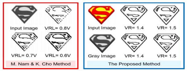
Nam M, Cho K (2018) Implementation of real-time image edge detector based on a bump circuit and active pixels in a CMOS image sensor. Integration 60: 56–62. doi: 10.1016/j.vlsi.2017.07.005
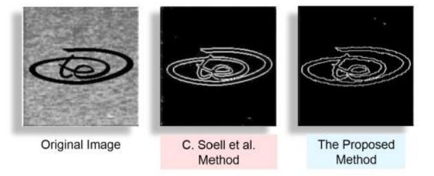
    [57] Soell C, Shi L, Roeber J, et al. (2016) Low-power analog smart camera sensor for edge detection. In: 2016 IEEE International Conference on Image Processing (ICIP), pp. 4408–4412.
    [58] Lee C, Chao W, Lee S, et al. (2015) A Low-Power Edge Detection Image Sensor Based on Parallel Digital Pulse Computation. IEEE Transactions on Circuits and Systems II: Express Briefs 62: 1043–1047. doi: 10.1109/TCSII.2015.2455354
    [59] 
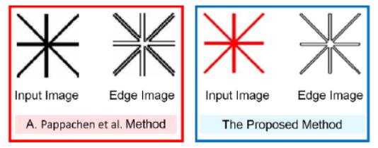
James A, Pachentavida A, Sugathan S (2014) Edge detection using resistive threshold logic networks with CMOS flash memories. International Journal of Intelligent Computing and Cybernetics 7: 79–94. doi: 10.1108/IJICC-06-2013-0032
  • This article has been cited by:

    1. Yaogan Liang, Bang Du, Kohei Nakamura, Shengwei Wang, Bunta Inoue, Yuta Aruga, Hisashi Kino, Takafumi Fukushima, Koji Kiyoyama, Tetsu Tanaka, 3D-stacked retinal prosthesis chip with binary image capture and edge detection functions for human visual restoration, 2022, 19, 1349-2543, 20220363, 10.1587/elex.19.20220363
    2. Anas Al Tarabsheh, Huda Alheeh, 2022, Design and Simulation of a 3-Transistor Active Pixel Sensor Using MATLAB Simulink, 979-8-3503-2024-4, 1, 10.1109/ACIT57182.2022.9994188
  • Reader Comments
  • © 2019 the Author(s), licensee AIMS Press. This is an open access article distributed under the terms of the Creative Commons Attribution License (http://creativecommons.org/licenses/by/4.0)
通讯作者: 陈斌, bchen63@163.com
  • 1. 

    沈阳化工大学材料科学与工程学院 沈阳 110142

  1. 本站搜索
  2. 百度学术搜索
  3. 万方数据库搜索
  4. CNKI搜索

Metrics

Article views(9781) PDF downloads(3218) Cited by(2)

Figures and Tables

Figures(24)  /  Tables(1)

Other Articles By Authors

/

DownLoad:  Full-Size Img  PowerPoint
Return
Return

Catalog