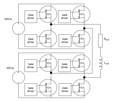
In this paper, the performance of a 5-level cascaded H-bridge inverter in unmanned aerial vehicle (UAV) applications is analized to identify, at the converter design stage, the better device choice depending on different UAV operation scenarios. Considering that regardless of the specific application there are some typical operations, such as take-off, climb, land, cruise, and potential recurring climbs and descents, the results can support the choice by considering the typical working conditions of the specific application where the UAV would be used. The results have been obtained by simulating the H-bridge inverter considering the circuit models of insulated-gate bipolar transistors (IGBTs), GaN high-electron-mobility transistors (HEMTs), and Si and SiC metal-oxide-semiconductor field-effect transistors (MOSFETs) provided by manufacturers. The study has highlighted that the choice of the device depends on the UAV usage, switching frequency, and load conditions. More specifically, considering the typical devices and systems costs in the case of a selective harmonic elimination procedure operating at the fundamental switching frequency, the Si devices should be used. Moreover, the preference for using IGBTs or Si MOSFETs depends on the typical working conditions of the UAV application. In the case of phase-shift carrier modulation technique, at 4 kHz the MOSFET is the best device and the choice between Si and SiC devices depends on the UAV application's main operation scenarios. At 20 kHz the SiC MOSFET is the best device, while at higher frequencies the GaN HEMT cost should be faced to take advantage of its best performance.
Citation: Enrico Alfredo Bottaro, Cristina Ventura, Santi Agatino Rizzo. Circuit simulation-based comparison of power electronics devices in a five-level converter for UAV applications[J]. AIMS Energy, 2024, 12(4): 905-923. doi: 10.3934/energy.2024042
In this paper, the performance of a 5-level cascaded H-bridge inverter in unmanned aerial vehicle (UAV) applications is analized to identify, at the converter design stage, the better device choice depending on different UAV operation scenarios. Considering that regardless of the specific application there are some typical operations, such as take-off, climb, land, cruise, and potential recurring climbs and descents, the results can support the choice by considering the typical working conditions of the specific application where the UAV would be used. The results have been obtained by simulating the H-bridge inverter considering the circuit models of insulated-gate bipolar transistors (IGBTs), GaN high-electron-mobility transistors (HEMTs), and Si and SiC metal-oxide-semiconductor field-effect transistors (MOSFETs) provided by manufacturers. The study has highlighted that the choice of the device depends on the UAV usage, switching frequency, and load conditions. More specifically, considering the typical devices and systems costs in the case of a selective harmonic elimination procedure operating at the fundamental switching frequency, the Si devices should be used. Moreover, the preference for using IGBTs or Si MOSFETs depends on the typical working conditions of the UAV application. In the case of phase-shift carrier modulation technique, at 4 kHz the MOSFET is the best device and the choice between Si and SiC devices depends on the UAV application's main operation scenarios. At 20 kHz the SiC MOSFET is the best device, while at higher frequencies the GaN HEMT cost should be faced to take advantage of its best performance.

| [1] |
Yang K, Feng M, Wang Y, et al. (2019) Real-time switching angle computation for selective harmonic control. IEEE Trans Power Electron 34: 8201–8212. https://doi.org/10.1109/TPEL.2018.2881448 doi: 10.1109/TPEL.2018.2881448

|
| [2] |
Faizan M, Wang X, Yousaf MZ (2023) Design and comparative analysis of an ultra-highly efficient, compact half-bridge LLC resonant GaN converter for low-power applications. Electronics 12: 2850. https://doi.org/10.3390/electronics12132850 doi: 10.3390/electronics12132850
|
| [3] |
Sun P, Zou M, Wang Y, et al. (2023) Focuses and concerns of dynamic test for wide bandgap device: A questionnaire-based survey. IEEE Trans Power Electron 38: 15522–15534. https://doi.org/10.1109/TPEL.2023.3312563 doi: 10.1109/TPEL.2023.3312563
|
| [4] |
Ilves K, Harnefors L, Norrga S, et al. (2015) Analysis and operation of modular multilevel converters with phase-shifted carrier PWM. IEEE Trans Power Electron 30: 268–283. https://doi.org/10.1109/TPEL.2014.2321049 doi: 10.1109/TPEL.2014.2321049
|
| [5] | Joshi V, Pande P, Jadli U, et al. (2023) Impact of parasitic elements on the power dissipation of Si superjunction MOSFETs, SiC MOSFETs, and GaN HEMTs. Eng Res Express 5: 035077. https://doi.org/10.1088/2631-8695/acf97d |
| [6] |
Zhong K, Wang Y, Lyu G, et al. (2022) 650-V normally-off GaN/SiC cascode device for power switching applications. IEEE Trans Ind Electron 69: 8997–9006. https://doi.org/10.1109/TIE.2021.3114697 doi: 10.1109/TIE.2021.3114697
|
| [7] | Sulistyo M, Pradhityo G, Muharam A, et al. (2023) Modeling high frequency 13.56 MHz Full bridge inverter based on GaN MOSFET for EV wireless charging system. Evergreen 10: 1847–1854. https://doi.org/10.5109/7151734 |
| [8] | Neeraja K, Bhavya Y, Mohan S, et al. (2016) Design, simulation and implementation techniques of high performance GaN SMPS. IEEE International Conference on Power Electronics, Drives and Energy Systems (PEDES), Trivandrum, India. https://doi.org/10.1109/PEDES.2016.7914396 |
| [9] | Zakzewski D, Resalayyan R, Hasnain A, et al. (2023) Controller verification of a smart-grid compatible 200 kHz single-stage photovoltaic microinverter. IEEE Applied Power Electronics Conference and Exposition (APEC), Orlando, FL, USA. https://doi.org/10.1109/APEC43580.2023.10131580 |
| [10] |
Isa R, Mirza J, Ghafoor S, et al. (2023) Junction temperature optical sensing techniques for power switching semiconductors: A review. Micromachines 14: 1636. https://doi.org/10.3390/mi14081636 doi: 10.3390/mi14081636
|
| [11] |
Hwang D, Joo D, Gu B (2024) Analysis of inverter loss improvement according to Si-IGBT and SiC-MOSFET utilization of 150kW inverter for EV propulsion. Trans Korean Inst Electr Eng 73: 63–68. https://doi.org/10.5370/KIEE.2024.73.1.63 doi: 10.5370/KIEE.2024.73.1.63
|
| [12] |
Li B, Yang R, Xu D, et al. (2015) Analysis of the phase-shifted carrier modulation for modular multilevel converters. IEEE Trans Power Electron 30: 297–310. https://doi.org/10.1109/TPEL.2014.2299802 doi: 10.1109/TPEL.2014.2299802
|
| [13] |
Villanueva I, Vázquez N, Vaquero J, et al. (2023) Photovoltaic inverter reliability study through sic switches redundant structures. Technologies 11: 59. https://doi.org/10.3390/technologies11020059 doi: 10.3390/technologies11020059
|
| [14] |
Alatise O, Deb A, Bashar E, et al. (2023) A review of power electronic devices for heavy goods vehicles electrification: performance and reliability. Energies 16: 4380. https://doi.org/10.3390/en16114380 doi: 10.3390/en16114380
|
| [15] | Carrasco-González D, Horrillo-Quintero P, García-Triviño P, et al. (2024). Control of PV power plants with quasi-Z-source cascaded H-bridge multilevel inverters under failure. Int Electr Power Energy Syst, 157. https://doi.org/10.1016/j.ijepes.2024.109803 |
| [16] | Sivarajeswari S, Hublikar S, Kumar Y, et al. (2024) Multiple level inverter scheme for improved power quality of renewable energy solar panel. Int J Intell Syst Appl Eng 12: 98–105. Available from: https://ijisae.org/index.php/IJISAE/article/view/3398. |
| [17] |
Gao S, Chen Y, Song Y, et al. (2024) An efficient half-bridge MMC model for emtp-type simulation based on hybrid numerical integration. IEEE Trans Power Syst 39: 1162–1177. https://doi.org/10.1109/TPWRS.2023.3262584 doi: 10.1109/TPWRS.2023.3262584
|
| [18] |
Sheng J, Xiang X, Li B, et al. (2023) High-Efficient operation for modular multilevel resonant DC–DC converters in medium voltage applications with wide input range and wide load condition. IEEE Trans Power Electron 38: 12180–12194. https://doi.org/10.1109/TPEL.2023.3295828 doi: 10.1109/TPEL.2023.3295828
|
| [19] |
Muthukaruppasamy S, Parimalasundar E, Rajagopal V, et al. (2023) Integrating MPPT and artificial neural networks for efficient DC-DC and DC-AC conversion in photovoltaic applications. SSRG Int J Electr Electron Eng 10: 51–61. https://doi.org/10.14445/23488379/IJEEE-V10I8P105 doi: 10.14445/23488379/IJEEE-V10I8P105
|
| [20] |
Babaie M, Al-Haddad K (2023) Self-Training intelligent predictive control for grid-tied transformerless multilevel converters. IEEE Trans Power Electron 38: 12482–12496. https://doi.org/10.1109/TPEL.2023.3293820 doi: 10.1109/TPEL.2023.3293820
|
| [21] |
Buccella C, Cecati C, Cimoroni M, et al. (2014) Analytical method for pattern generation in five-level cascaded H-bridge inverter using selective harmonic elimination. IEEE Trans Ind Electron 61: 5811–5819. https://doi.org/10.1109/TIE.2014.2308163 doi: 10.1109/TIE.2014.2308163
|
| [22] | Dutta S, Yadav A (2023) Power loss comparison of Si-IGBT SiC-MOSFET and GaN Based 3-level diode clamped inverter fed induction motor drive. IEEE International Conference on Power Electronics, Smart Grid, and Renewable Energy (PESGRE), Trivandrum, India. https://doi.org/10.1109/PESGRE58662.2023.10405187 |
| [23] | Liu Y, Ge B, Abu-Rub H, et al. (2016) Comparison of SiC and GaN devices for front-end isolation of quasi-Z-source cascaded multilevel photovoltaic inverter. IEEE Energy Conversion Congress and Exposition (ECCE), Milwaukee, WI, USA. https://doi.org/10.1109/ECCE.2016.7854942 |
| [24] | Najjar M, Nymand M, Kouchaki A, et al. (2021) Efficiency comparisons of two-level and three-level GaN/SiC based converters. IEEE 12th Energy Conversion Congress & Exposition—Asia (ECCE-Asia), Singapore, 13–18. https://doi.org/10.1109/ECCE-Asia49820.2021.9479380 |
| [25] | Suryawanshi A, Chopade N, Mehta H (2021) Micro-controllers and power devices used in multilevel inverters—A Survey. International Conference on Green Energy, Computing and Sustainable Technology (GECOST), Miri, Malaysia, 1–5. https://doi.org/10.1109/GECOST52368.2021.9538707 |
| [26] |
Buccella C, Cecati C, Cimoroni M, et al. (2017) A selective harmonic elimination method for five-level converters for distributed generation. IEEE J Emerg Select Topic Pow Elec 5: 775–783. https://doi.org/10.1109/JESTPE.2017.2688726 doi: 10.1109/JESTPE.2017.2688726
|
| [27] | Spice model of the device STO67N60DM6. Available from: https://www.st.com/resource/en/spice_model/sto67n60dm6_spice.zip. |
| [28] | Spice model of the device IMZA65R048M1H. Available from: https://www.infineon.com/dgdl/Infineon-CoolSiC_silicon_carbide_MOSFET_650V_SPICE-SimulationModels-v05_00-EN.zip?fileId = 5546d4626fc1ce0b016fc742477d0bb1. |
| [29] | Spice model of the device GS-065-030-2-L. Available from: https://gansystems.com/wp-content/uploads/2021/08/GS-650-030-2-L-Spice-Models-V3P2.rar. |
| [30] | Spice model of the device STGWA60V60DWFAG. Available from: https://www.st.com/en/power-transistors/stgwa60v60dwfag.html#cad-resources. |
| [31] | What is the recommended gate resistance to start with? Available from: https://gansystems.com/gan-transistors/faq/#toggle-id-12. |
| [32] |
Zarębski J, Bisewski D (2023) The modeling of GaN-FET power devices in SPICE. Energies 16: 7643. https://doi.org/10.3390/en16227643 doi: 10.3390/en16227643
|
| [33] | Er-Rafii H, Galadi A (2023) An optimal parameter extraction procedure for SiC power MOSFET Model. J Integr Circuits Syst, 18. https://doi.org/10.29292/jics.v18i2.756 |
| [34] |
Pan Z, Liu Y, Ren D, et al. (2023) A MOSFET EMC modeling method based on electrical characteristic measurement and simplex optimization and particle swarm optimization. Int J Circ Theor Appl 6: 2936–2955. https://doi.org/10.1002/cta.3856 doi: 10.1002/cta.3856
|
| [35] | Borghese A, Riccio M, Maresca L, et al. (2023) A scalable SPICE electrothermal compact model for SiC MOSFETs: A comparative study between the LEVEL-3 and the BSIM. Key Eng Mater 947. https://doi.org/10.4028/p-hmxz8o |
| [36] | Cusumano A, Crimi D, Raffa A, et al. (2023) SPICE-based model validation for 1200 V AcepackTM Drive traction power module. International Symposium on Electromagnetic Compatibility—EMC Europe, Krakow, Poland. https://doi.org/10.1109/EMCEurope57790.2023.10274154 |
| [37] |
Bottaro E, Rizzo S (2023) An overview of strengths and weaknesses in using MOSFET experience for modeling GaN HEMT. Energies 16: 6574. https://doi.org/10.3390/en16186574 doi: 10.3390/en16186574
|


Figures(13) / Tables(4)

Enrico Alfredo Bottaro, Cristina Ventura, Santi Agatino Rizzo. Circuit simulation-based comparison of power electronics devices in a five-level converter for UAV applications[J]. AIMS Energy, 2024, 12(4): 905-923. doi: 10.3934/energy.2024042


 DownLoad: