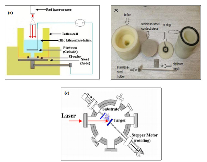
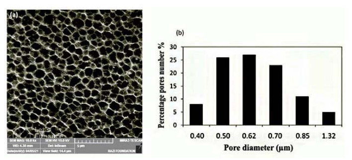
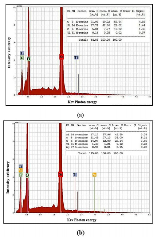
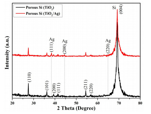
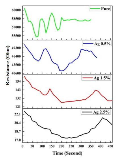
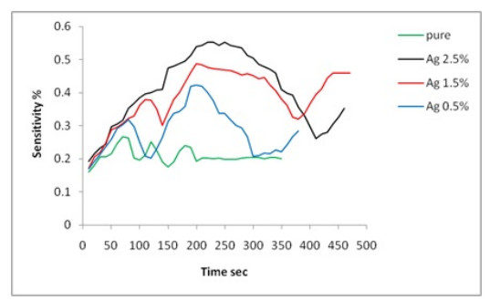
In this research, two pellets of titanium dioxide TiO2 were prepared at room temperature. The first was pure titanium dioxide, and the other was doped with silver (2.5%). The pellets were deposited on porous silicon (PSi) with the pulsed laser deposition (PLD) technique. The results of scanning electron microscopy and energy-dispersive X-ray spectroscopy showed improvements in the surface morphologies of the TiO2/PSi and TiO2@Ag/PSi composites. The composites were then tested as CO2 gas sensors. The electrical measurements of the composites showed a decrease in the electrical resistance of the CO2 gas sensor doped with a metal. Sensitivity to CO2 increased to up to 55% in Ag-doped TiO2 film with a concentration of 2.5%, and the highest sensitivity value was obtained in the pure titanium dioxide film (26%).
Citation: Ahmed Z. Abdullah, Adawiya J. Haider, Allaa A. Jabbar. Pure TiO2/PSi and TiO2@Ag/PSi structures as controllable sensor for toxic gases[J]. AIMS Materials Science, 2022, 9(4): 522-533. doi: 10.3934/matersci.2022031
In this research, two pellets of titanium dioxide TiO2 were prepared at room temperature. The first was pure titanium dioxide, and the other was doped with silver (2.5%). The pellets were deposited on porous silicon (PSi) with the pulsed laser deposition (PLD) technique. The results of scanning electron microscopy and energy-dispersive X-ray spectroscopy showed improvements in the surface morphologies of the TiO2/PSi and TiO2@Ag/PSi composites. The composites were then tested as CO2 gas sensors. The electrical measurements of the composites showed a decrease in the electrical resistance of the CO2 gas sensor doped with a metal. Sensitivity to CO2 increased to up to 55% in Ag-doped TiO2 film with a concentration of 2.5%, and the highest sensitivity value was obtained in the pure titanium dioxide film (26%).

| [1] | Korotcenkov G (2016) Optoelectronics, microelectronics, and energy technology applications, Porous Silicon: From Formation to Applications, CRC Press. |
| [2] | Canham LT (1997) Properties of Porous Silicon, London: Inst of Engineering & Technology. |
| [3] | Haider AJ (2008) The effect of some experimental parameters on the properties of porous silicon. IJAP 4: 37–40. |
| [4] |
Haider AJ, Al-Anbari R, Sami HM, et al. (2019) Enhance preparation and characterization of nickel-oxide as self-cleaning surfaces. Energ Procedia 157: 1328–1342. https://doi.org/10.1016/j.egypro.2018.11.298 doi: 10.1016/j.egypro.2018.11.298

|
| [5] |
Parkhutik V (1999) Porous silicon-mechanisms of growth and applications. Solid State Electron 43: 1121–1141. https://doi.org/10.1016/S0038-1101(99)00036-2 doi: 10.1016/S0038-1101(99)00036-2
|
| [6] |
Jabbar AA, Haider AJ, Haider MJ, et al. (2020) Preparation and characterization of NiO/PSi as self-cleaning surface. J Mater Res Technol 9: 15123–15131. https://doi.org/10.1016/j.jmrt.2020.10.075 doi: 10.1016/j.jmrt.2020.10.075
|
| [7] | Sailor MJ (2012) Porous Silicon in Practice: Preparation, Characterization and Applications, John Wiley & Sons. https://doi.org/10.1002/9783527641901 |
| [8] |
Goryachev D, Belyakov L, Sreseli O (2003) Electrolytic fabrication of porous silicon with the use of internal current source. Semiconductors 37: 477–481. https://doi.org/10.1134/1.1568472 doi: 10.1134/1.1568472
|
| [9] |
Lang W (1996) Silicon microstructuring technology. Mater Sci Eng R 17: 1–55. https://doi.org/10.1016/0927-796X(96)00190-8 doi: 10.1016/0927-796X(96)00190-8
|
| [10] |
Bomchil G, Halimaoui A, Herino R (1988) Porous silicon: the material and its applications to SOI technologies. Microelectron Eng 8: 293–310. https://doi.org/10.1016/0167-9317(88)90022-6 doi: 10.1016/0167-9317(88)90022-6
|
| [11] |
Bisi O, Ossicini S, Pavesi L (2000) Porous silicon: a quantum sponge structure for silicon based optoelectronics. Surf Sci Rep 38: 1–126. https://doi.org/10.1016/S0167-5729(99)00012-6 doi: 10.1016/S0167-5729(99)00012-6
|
| [12] |
AA Salih, AJ Haider, A Nazar (2020) Preparation and characterizations of nanomaterial by pulsed laser ablation in liquid (PLAIL) as friendly environment paint. J Phys Conf Ser 1795: 012023. https://doi.org/10.1088/1742-6596/1795/1/012023 doi: 10.1088/1742-6596/1795/1/012023
|
| [13] |
Ozdemir S, Gole JL (2007) The potential of porous silicon gas sensors. Curr Opin Solid St M 11: 92–100. https://doi.org/10.1016/j.cossms.2008.06.003 doi: 10.1016/j.cossms.2008.06.003
|
| [14] | Carpenter MA, Mathur S, Kolmakov A (2012) Metal Oxide Nanomaterials for Chemical Sensors, Springer Science & Business Media. https://doi.org/10.1007/978-1-4614-5395-6 |
| [15] |
Manjakkal L, Szwagierczak D, Dahiya R (2020) Metal oxides based electrochemical pH sensors: Current progress and future perspectives. Prog Mater Sci 109: 100635. https://doi.org/10.1016/j.pmatsci.2019.100635 doi: 10.1016/j.pmatsci.2019.100635
|
| [16] |
Saleh AA, Haider AJ, Nazar A (2021) Preparation and properties of mattel oxide nanoparticles by pulse laser ablation in liquid as photo-catalysis. Key Eng Mater 900: 197–204. https://doi.org/10.4028/www.scientific.net/KEM.900.197 doi: 10.4028/www.scientific.net/KEM.900.197
|
| [17] | Abed AL, Mohammed FQ, Hasan AS (2017) Synthesis and study of modified nanostructure porous silicon layers for chemical gas sensing. Eng Technol J 35: 970–974. |
| [18] |
Kahdim GR, AL-Anbari RH, Haider AJ (2018) Preparation and characterization of TiO2 nanoparticles and its applications as antibacterial agents. Eng Technol J 36: 1068–1074. https://doi.org/10.30684/etj.36.10A.7 doi: 10.30684/etj.36.10A.7
|
| [19] |
Navale S, Shahbaz M, Mirzaei A, et al. (2021) Effect of Ag addition on the gas-sensing properties of nanostructured resistive-based gas sensors: An overview. Sensors 21: 6454. https://doi.org/10.3390/s21196454 doi: 10.3390/s21196454
|
| [20] |
El-Sayet A, Ismail F, Yakout S (2011) Electrical conductivity and sensitive characteristics of Ag-added BaTiO3-CuO mixed oxide for CO2 gas sensing. J Mater Sci Technol 27: 35–40. https://doi.org/10.1016/S1005-0302(11)60022-4 doi: 10.1016/S1005-0302(11)60022-4
|
| [21] | Alwan AM (2014) An investigation of multi-porous silicon gas sensor. Eng Technol J 32: 183–190. |
| [22] | Basu S (2011) Crystalline Silicon: Properties and Uses, BoD-Books on Demand. https://doi.org/10.5772/844 |
| [23] |
Hwang J, Hwang S, Chou C, et al. (2011) Investigation of opto-electronic properties on gradient-porosity porous silicon layer. Thin Solid Films 519: 2313–2316. https://doi.org/10.1016/j.tsf.2010.11.041 doi: 10.1016/j.tsf.2010.11.041
|
| [24] |
Haider AJ, Jabbar AA, Ali GA (2021) A review of pure and doped ZnO nanostructure production and its optical properties using pulsed laser deposition technique. J Phys Conf Ser 1795: 012015. https://doi.org/10.1088/1742-6596/1795/1/012015 doi: 10.1088/1742-6596/1795/1/012015
|
| [25] |
Haider AJ, Al-Kinani MA, Al-Musawi S (2021) Preparation and characterization of gold coated super paramagnetic iron nanoparticle using pulsed laser ablation in liquid method. Key Eng Mater 886: 77–85. https://doi.org/10.4028/www.scientific.net/KEM.886.77 doi: 10.4028/www.scientific.net/KEM.886.77
|
| [26] | Carlsson JM (2010) Simulations of the structural and chemical properties of nanoporous carbon, In: Colombo L, Fasolino A, Computer-Based Modeling of Novel Carbon Systems and Their Properties, Springer, 79–128. https://doi.org/10.1007/978-1-4020-9718-8_4 |
| [27] |
Hadi HA, Ismail RA, Habubi NF (2013) Fabrication and characterization of porous silicon layer prepared by photo-electrochemical etching in CH3OH: HF solution. ILCPA 3: 29–36. https://doi.org/10.18052/www.scipress.com/ILCPA.8.29 doi: 10.18052/www.scipress.com/ILCPA.8.29
|
| [28] |
Maniya NH, Patel SR, Murthy Z (2013) Electrochemical preparation of microstructured porous silicon layers for drug delivery applications. Superlattice Microst 55: 144–150. https://doi.org/10.1016/j.spmi.2012.12.005 doi: 10.1016/j.spmi.2012.12.005
|
| [29] |
Mogal SI, Mishra M, Gandhi VG, et al. (2013) Metal doped titanium dioxide: synthesis and effect of metal ions on physico-chemical and photocatalytic properties. Mater Sci Forum 734: 364–378. https://doi.org/10.4028/www.scientific.net/MSF.734.364 doi: 10.4028/www.scientific.net/MSF.734.364
|
| [30] | Korotcenkov G (2013) Conventional approaches, Handbook of Gas Sensor Materials, Springer. https://doi.org/10.1007/978-1-4614-7165-3 |
| [31] |
Mariappan R, Ponnuswamy V, Suresh P, et al. (2014) Influence of film thickness on the properties of sprayed ZnO thin films for gas sensor applications. Superlattice Microst 71: 238–249. https://doi.org/10.1016/j.spmi.2014.03.029 doi: 10.1016/j.spmi.2014.03.029
|
| [32] | Faburada AL (1978) The Effects of Electron-donating and Electron-with Drawing Groups on the Alkylation Sites of Para-substituted Phenylacetones, Western Michigan University ProQuest Dissertations Publishing. |
| [33] | Haider AJ, Mutasher HA (2015) A study on the structural, optical and electrical properties of tungsten trioxideWO3 thin film for gas sensing applications. Eng Technol J 33: 1473–1482. |
| [34] |
Sheini NA, Rohani M (2016) Ag-doped titanium dioxide gas sensor. IOP Conf Ser Mater Sci Eng 108: 012033. https://doi.org/10.1088/1757-899X/108/1/012033 doi: 10.1088/1757-899X/108/1/012033
|
| [35] |
Ramesan M, Santhi V, Bahuleyan B, et al. (2018) Structural characterization, material properties and sensor application study of in situ polymerized polypyrrole/silver doped titanium dioxide nanocomposites. Mater Chem Phys 211: 343–354. https://doi.org/10.1016/j.matchemphys.2018.02.040 doi: 10.1016/j.matchemphys.2018.02.040
|

Figures(7) / Tables(1)

Ahmed Z. Abdullah, Adawiya J. Haider, Allaa A. Jabbar. Pure TiO2/PSi and TiO2@Ag/PSi structures as controllable sensor for toxic gases[J]. AIMS Materials Science, 2022, 9(4): 522-533. doi: 10.3934/matersci.2022031


 DownLoad: